参数资料
| 型号: | LT3085EMS8E#PBF |
| 厂商: | Linear Technology |
| 文件页数: | 15/28页 |
| 文件大小: | 0K |
| 描述: | IC REG LDO ADJ .5A 8-MSOP |
| 产品培训模块: | LT3085 Adjustable Low Dropout Regulator More Information on LDOs |
| 标准包装: | 50 |
| 稳压器拓扑结构: | 正,可调式 |
| 输出电压: | 可调 |
| 输入电压: | 1.2 V ~ 36 V |
| 电压 - 压降(标准): | 1.35V @ 500mA |
| 稳压器数量: | 1 |
| 电流 - 输出: | 500mA |
| 电流 - 限制(最小): | 500mA |
| 工作温度: | -40°C ~ 125°C |
| 安装类型: | 表面贴装 |
| 封装/外壳: | 8-TSSOP,8-MSOP(0.118",3.00mm 宽)裸露焊盘 |
| 供应商设备封装: | 8-MSOP-EP |
| 包装: | 管件 |
| 产品目录页面: | 1331 (CN2011-ZH PDF) |
第1页第2页第3页第4页第5页第6页第7页第8页第9页第10页第11页第12页第13页第14页当前第15页第16页第17页第18页第19页第20页第21页第22页第23页第24页第25页第26页第27页第28页
�� �
�
�LT3085�
�APPLICATIONS� INFORMATION�
�If� the� LT3085� is� con?gured� as� a� three-terminal� (single� supply)�
�regulator� with� IN� and� V� CONTROL� shorted� together,� the� internal�
�diode� of� the� IN� pin� will� protect� the� V� CONTROL� pin.�
�Like� any� other� regulator,� exceeding� the� maximum� input-�
�to-output� differential� causes� internal� transistors� to� break�
�down� and� then� none� of� the� internal� protection� circuitry�
�is� functional.�
�Thermal� Considerations�
�provide� better� performance� than� found� in� these� tables.�
�For� example,� a� 4-layer,� 1� ounce� copper� PCB� board� with�
�5� thermal� vias� from� the� DFN� or� MSOP� exposed� backside�
�pad� to� inner� layers� (connected� to� V� OUT� )� achieves� 40°C/W�
�thermal� resistance.� Demo� circuit� 1401A’s� board� layout�
�achieves� this� 40°C/W� performance.� This� is� approximately�
�a� 45%� improvement� over� the� numbers� shown� in� Tables�
�2� and� 3.�
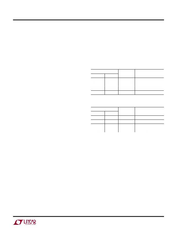
�Table� 2.� MSE� Package,� 8-Lead� MSOP�
�The� LT3085� has� internal� power� and� thermal� limiting� cir-�
�COPPER� AREA�
�THERMAL� RESISTANCE�
�cuitry� designed� to� protect� it� under� overload� conditions.�
�For� continuous� normal� load� conditions,� maximum� junc-�
�tion� temperature� must� not� be� exceeded.� It� is� important�
�to� give� consideration� to� all� sources� of� thermal� resistance�
�from� junction� to� ambient.� This� includes� junction-to-case,�
�TOPSIDE*�
�2500mm� 2�
�1000mm� 2�
�225mm� 2�
�100mm� 2�
�BACKSIDE�
�2500mm� 2�
�2500mm� 2�
�2500mm� 2�
�2500mm� 2�
�BOARD� AREA�
�2500mm� 2�
�2500mm� 2�
�2500mm� 2�
�2500mm� 2�
�(JUNCTION-TO-AMBIENT)�
�55°C/W�
�57°C/W�
�60°C/W�
�65°C/W�
�case-to-heat� sink� interface,� heat� sink� resistance� or� circuit�
�board-to-ambient� as� the� application� dictates.� Additional�
�heat� sources� nearby� must� also� be� considered.�
�*Device� is� mounted� on� topside�
�Table� 3.� DCB� Package,� 6-Lead� DFN�
�For� surface� mount� devices,� heat� sinking� is� accomplished�
�by� using� the� heat� spreading� capabilities� of� the� PC� board�
�and� its� copper� traces.� Surface� mount� heat� sinks� and�
�plated� through-holes� can� also� be� used� to� spread� the� heat�
�generated� by� power� devices.� Boards� speci?ed� in� thermal�
�resistance� tables� have� no� vias� on� plated� through-holes�
�COPPER� AREA�
�TOPSIDE*� BACKSIDE�
�2500mm� 2� 2500mm� 2�
�1000mm� 2� 2500mm� 2�
�225mm� 2� 2500mm� 2�
�100mm� 2� 2500mm� 2�
�BOARD� AREA�
�2500mm� 2�
�2500mm� 2�
�2500mm� 2�
�2500mm� 2�
�THERMAL� RESISTANCE�
�(JUNCTION-TO-AMBIENT)�
�68°C/W�
�70°C/W�
�73°C/W�
�78°C/W�
�from� topside� to� backside.�
�Junction-to-case� thermal� resistance� is� speci?ed� from�
�the� IC� junction� to� the� bottom� of� the� case� directly� below�
�the� die.� This� is� the� lowest� resistance� path� for� heat� ?ow.�
�Proper� mounting� is� required� to� ensure� the� best� possible�
�thermal� ?ow� from� this� area� of� the� package� to� the� heat�
�sinking� material.� Note� that� the� Exposed� Pad� is� electrically�
�connected� to� the� output.�
�The� following� tables� list� thermal� resistance� for� several�
�different� copper� areas� given� a� ?xed� board� size.� All� mea-�
�surements� were� taken� in� still� air� on� two-sided� 1/16”� FR-4�
�board� with� one� ounce� copper.�
�PCB� layers,� copper� weight,� board� layout� and� thermal� vias�
�affect� the� resultant� thermal� resistance.� Although� Tables�
�2� and� 3� provide� thermal� resistance� numbers� for� 2-layer�
�board� with� 1� ounce� copper,� modern� multi-layer� PCBs�
�*Device� is� mounted� on� topside�
�For� future� information� on� the� thermal� resistance� and� using� thermal�
�information,� refer� to� JEDEC� standard� JESD51,� notably� JESD51-12.�
�Calculating� Junction� Temperature�
�Example:� Given� an� output� voltage� of� 0.9V,� a� V� CONTROL�
�voltage� of� 3.3V� ±10%,� an� IN� voltage� of� 1.5V� ±5%,� output�
�current� range� from� 1mA� to� 0.5A� and� a� maximum� ambi-�
�ent� temperature� of� 50°C,� what� will� the� maximum� junction�
�temperature� be� for� the� DFN� package� on� a� 2500mm� 2� board�
�with� topside� copper� area� of� 500mm� 2� ?�
�The� power� in� the� drive� circuit� equals:�
�P� DRIVE� =� (V� CONTROL� –� V� OUT� )(I� CONTROL� )�
�where� I� CONTROL� is� equal� to� I� OUT� /60.� I� CONTROL� is� a� function�
�of� output� current.� A� curve� of� I� CONTROL� vs� I� OUT� can� be� found�
�in� the� Typical� Performance� Characteristics� curves.�
�3085fb�
�15�
�相关PDF资料 |
PDF描述 |
|---|---|
| LT1121IS8-5#PBF | IC REG LDO 5V .15A 8-SOIC |
| HMC17DRTI-S13 | CONN EDGECARD 34POS .100 EXTEND |
| RSC12DTES | CONN EDGECARD 24POS .100 EYELET |
| EMM28DTMS | CONN EDGECARD 56POS R/A .156 SLD |
| HSC22DRES-S13 | CONN EDGECARD 44POS .100 EXTEND |
相关代理商/技术参数 |
参数描述 |
|---|---|
| LT3085EMS8E-TR | 制造商:LINER 制造商全称:Linear Technology 功能描述:Adjustable 500mA Single Resistor Low Dropout Regulator |
| LT3085EMS8E-TRPBF | 制造商:LINER 制造商全称:Linear Technology 功能描述:Adjustable 500mA Single Resistor Low Dropout Regulator |
| LT3085IDCB | 制造商:LINER 制造商全称:Linear Technology 功能描述:Adjustable 500mA Single Resistor Low Dropout Regulator |
| LT3085IDCB#PBF | 制造商:Linear Technology 功能描述:LDO Regulator Pos 0V to 36V 0.5A 6-Pin DFN EP 制造商:Linear Technology 功能描述:LDO Regulator Pos 0V to 36V 0.5A 6-Pin DFN EP Bulk |
| LT3085IDCB#TRMPBF | 功能描述:IC REG LDO ADJ .5A 6-DFN RoHS:是 类别:集成电路 (IC) >> PMIC - 稳压器 - 线性 系列:- 标准包装:800 系列:- 稳压器拓扑结构:正,固定式 输出电压:2.5V 输入电压:最高 16V 电压 - 压降(标准):0.7V @ 4A 稳压器数量:1 电流 - 输出:4A 电流 - 限制(最小):4.2A 工作温度:0°C ~ 125°C 安装类型:表面贴装 封装/外壳:TO-263-6,D²Pak(5 引线+接片),TO-263BA 供应商设备封装:TO-263-5 包装:带卷 (TR) 其它名称:AP1184K525L-13AP1184K525LDITR |
发布紧急采购,3分钟左右您将得到回复。