- 您现在的位置:买卖IC网 > PDF目录44983 > LT3430IFE-1#TR (LINEAR TECHNOLOGY CORP) 6.5 A SWITCHING REGULATOR, 120 kHz SWITCHING FREQ-MAX, PDSO16 PDF资料下载
参数资料
| 型号: | LT3430IFE-1#TR |
| 厂商: | LINEAR TECHNOLOGY CORP |
| 元件分类: | 稳压器 |
| 英文描述: | 6.5 A SWITCHING REGULATOR, 120 kHz SWITCHING FREQ-MAX, PDSO16 |
| 封装: | 4.40 MM, PLASTIC, TSSOP-16 |
| 文件页数: | 13/28页 |
| 文件大小: | 321K |
| 代理商: | LT3430IFE-1#TR |
第1页第2页第3页第4页第5页第6页第7页第8页第9页第10页第11页第12页当前第13页第14页第15页第16页第17页第18页第19页第20页第21页第22页第23页第24页第25页第26页第27页第28页
LT3430/LT3430-1
20
34301fa
lower VIN may generate greater losses due to switch DC
losses. In general, the maximum and minimum VIN levels
should be checked with maximum typical load current for
calculation of the LT3430/LT3430-1 die temperature. If a
more accurate die temperature is required, a measure-
ment of the SYNC pin resistance (to GND) can be used.
The SYNC pin resistance can be measured by forcing a
voltage no greater than 0.5V at the pin and monitoring the
pin current over temperature in an oven. This should be
done with minimal device power (low VIN and no switching
(VC = 0V)) in order to calibrate SYNC pin resistance with
ambient (oven) temperature.
Note: Some of the internal power dissipation in the IC,
due to BOOST pin voltage, can be transferred outside
of the IC to reduce junction temperature, by increasing
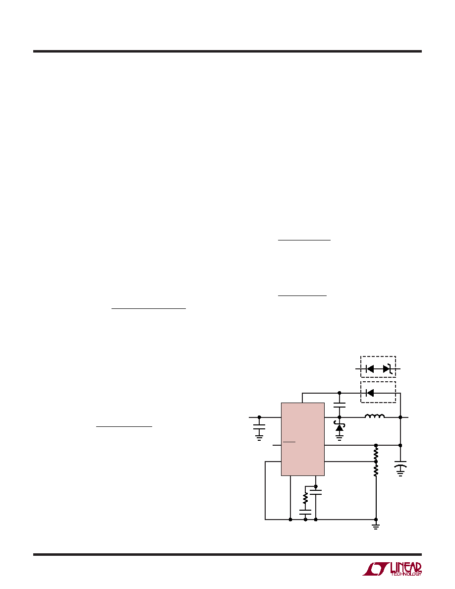
the voltage drop in the path of the boost diode D2 (see
Figure 9). This reduction of junction temperature inside
the IC will allow higher ambient temperature operation for
a given set of conditions. BOOST pin circuitry dissipates
power given by:
P
VI
V
DISS
OUT
SW
C
IN
BOOST Pin
=
()
/
36
2
Typically VC2 (the boost voltage across the capacitor C2)
equals VOUT. This is because diodes D1 and D2 can be
considered almost equal, where:
VC2 = VOUT – VFD2 – (–VFD1) = VOUT
Hence the equation used for boost circuitry power dissi-
pation given in the previous Thermal Calculations section
is stated as:
P
VI
V
DISS BOOST
OUT
SW
IN
OUT
()
/
=
()
36
Here it can be seen that boost power dissipation increases
as the square of VOUT. It is possible, however, to reduce
VC2 below VOUT to save power dissipation by increasing the
voltage drop in the path of D2. Care should be taken that
VC2 does not fall below the minimum 3.3V boost voltage
required for full saturation of the internal power switch.
For output voltages of 5V, VC2 is approximately 5V. During
switch turn on, VC2 will fall as the boost capacitor C2 is
dicharged by the BOOST pin. In the previous BOOST Pin
section, the value of C2 was designed for a 0.7V droop in
VC2 = VDROOP. Hence, an output voltage as low as 4V would
still allow the minimum 3.3V for the boost function using
the C2 capacitor calculated. If a target output voltage of
12V is required, however, an excess of 8V is placed across
the boost capacitor which is not required for the boost
function but still dissipates additional power.
What is required is a voltage drop in the path of D2 to
achieve minimal power dissipation while still maintaining
minimum boost voltage across C2. A zener, D4, placed in
series with D2 (see Figure 9), drops voltage to C2.
Example : the BOOST pin power dissipation for a 20V input
to 12V output conversion at 2A is given by:
PW
BOOST
=
()
=
12 2 36 12
20
04
/
.
If a 7V zener D4 is placed in series with D2, then power
dissipation becomes :
PW
BOOST
=
()
=
12 2 36 5
20
0 167
/
.
For an FE package with thermal resistance of 45°C/W,
ambient temperature savings would be, T(ambient) sav-
APPLICATIONS INFORMATION
BOOST
VIN
D1
R1
VOUT
CF
CC
LT3430/
LT3430-1
SHDN
SYNC
SW
BIAS
FB
VC
GND
C2
C1
L1
D2
R2
3430 F09
C3
VIN
D2
D4
+
RC
Figure 9. BOOST Pin, Diode Selection
相关PDF资料 |
PDF描述 |
|---|---|
| LT3430EFE-1#TR | 6.5 A SWITCHING REGULATOR, 120 kHz SWITCHING FREQ-MAX, PDSO16 |
| LT3430IFE-1 | 6.5 A SWITCHING REGULATOR, 120 kHz SWITCHING FREQ-MAX, PDSO16 |
| LT3430EFE-1 | 6.5 A SWITCHING REGULATOR, 120 kHz SWITCHING FREQ-MAX, PDSO16 |
| LT3467AIDDB#PBF | 2.5 A SWITCHING REGULATOR, 2700 kHz SWITCHING FREQ-MAX, PDSO8 |
| LT3467AIDDB | 2.5 A SWITCHING REGULATOR, 2700 kHz SWITCHING FREQ-MAX, PDSO8 |
相关代理商/技术参数 |
参数描述 |
|---|---|
| LT3430IFEPBF | 制造商:Linear Technology 功能描述:Sw. Regulator 3A 200kHz 60V TSSOP16EP |
| LT3431 | 制造商:LINER 制造商全称:Linear Technology 功能描述:High Voltage, 3A,500kHz Step-Down Switching Regulator |
| LT3431EFE | 功能描述:IC REG BUCK ADJ 3A 16TSSOP RoHS:否 类别:集成电路 (IC) >> PMIC - 稳压器 - DC DC 开关稳压器 系列:- 设计资源:Design Support Tool 标准包装:1 系列:- 类型:升压(升压) 输出类型:固定 输出数:1 输出电压:3V 输入电压:0.75 V ~ 2 V PWM 型:- 频率 - 开关:- 电流 - 输出:100mA 同步整流器:是 工作温度:-40°C ~ 85°C 安装类型:表面贴装 封装/外壳:SOT-23-5 细型,TSOT-23-5 包装:剪切带 (CT) 供应商设备封装:TSOT-23-5 其它名称:AS1323-BTTT-30CT |
| LT3431EFE#PBF | 功能描述:IC REG BUCK ADJ 3A 16TSSOP RoHS:是 类别:集成电路 (IC) >> PMIC - 稳压器 - DC DC 开关稳压器 系列:- 标准包装:250 系列:- 类型:降压(降压) 输出类型:固定 输出数:1 输出电压:1.2V 输入电压:2.05 V ~ 6 V PWM 型:电压模式 频率 - 开关:2MHz 电流 - 输出:500mA 同步整流器:是 工作温度:-40°C ~ 85°C 安装类型:表面贴装 封装/外壳:6-UFDFN 包装:带卷 (TR) 供应商设备封装:6-SON(1.45x1) 产品目录页面:1032 (CN2011-ZH PDF) 其它名称:296-25628-2 |
| LT3431EFE#TR | 功能描述:IC REG BUCK ADJ 3A 16TSSOP RoHS:否 类别:集成电路 (IC) >> PMIC - 稳压器 - DC DC 开关稳压器 系列:- 设计资源:Design Support Tool 标准包装:1 系列:- 类型:升压(升压) 输出类型:固定 输出数:1 输出电压:3V 输入电压:0.75 V ~ 2 V PWM 型:- 频率 - 开关:- 电流 - 输出:100mA 同步整流器:是 工作温度:-40°C ~ 85°C 安装类型:表面贴装 封装/外壳:SOT-23-5 细型,TSOT-23-5 包装:剪切带 (CT) 供应商设备封装:TSOT-23-5 其它名称:AS1323-BTTT-30CT |
发布紧急采购,3分钟左右您将得到回复。