- 您现在的位置:买卖IC网 > PDF目录13837 > LT3431IFE#TR (Linear Technology)IC REG BUCK ADJ 3A 16TSSOP PDF资料下载
参数资料
| 型号: | LT3431IFE#TR |
| 厂商: | Linear Technology |
| 文件页数: | 20/28页 |
| 文件大小: | 0K |
| 描述: | IC REG BUCK ADJ 3A 16TSSOP |
| 标准包装: | 2,500 |
| 类型: | 降压(降压) |
| 输出类型: | 可调式 |
| 输出数: | 1 |
| 输出电压: | 1.2 V ~ 48 V |
| 输入电压: | 5.5 V ~ 60 V |
| PWM 型: | 电流模式 |
| 频率 - 开关: | 500kHz |
| 电流 - 输出: | 3A |
| 同步整流器: | 无 |
| 工作温度: | -40°C ~ 125°C |
| 安装类型: | 表面贴装 |
| 封装/外壳: | 16-TSSOP(0.173",4.40mm)裸露焊盘 |
| 包装: | 带卷 (TR) |
| 供应商设备封装: | 16-TSSOP-EP |
第1页第2页第3页第4页第5页第6页第7页第8页第9页第10页第11页第12页第13页第14页第15页第16页第17页第18页第19页当前第20页第21页第22页第23页第24页第25页第26页第27页第28页
�� �
�
�LT3431�
�APPLICATIO� S� I� FOR� ATIO�
�Note:� Some� of� the� internal� power� dissipation� in� the� IC,� due�
�to� BOOST� pin� voltage,� can� be� transferred� outside� of� the� IC�
�Example� :� The� BOOST� pin� power� dissipation� for� a� 20V� input�
�to� 12V� output� conversion� at� 2A� is� given� by� :�
�to� reduce� junction� temperature,� by� increasing� the� voltage�
�drop� in� the� path� of� the� boost� diode� D2.� (see� Figure� 9).� This�
�reduction� of� junction� temperature� inside� the� IC� will� allow�
�P� BOOST� =�
�12 ? (2 / 36) ? 12�
�20�
�=� 0� .� 4� W�
�P� DISS� (� BOOST� )� =�
�P� BOOST� =�
�=� 0� .� 167� W�
�higher ambient temperature operation for a given set of�
�conditions.� BOOST� pin� circuitry� dissipates� power� given�
�by:�
�V� OUT� ? (I� SW� / 36) ? V� C 2�
�V� IN�
�Typically� V� C2� (the� boost� voltage� across� the� capacitor� C2)�
�equals� V� OUT� .� This� is� because� diodes� D1� and� D2� can� be�
�considered� almost� equal,� where:�
�V� C2� =� V� OUT� –� V� FD2� –� (–V� FD1� )� =� V� OUT� .�
�Hence� the� equation� used� for� boost� circuitry� power� dissipa-�
�tion� given� in� the� previous� Thermal� Calculations� section� is�
�stated� as:�
�If� a� 7V� zener� D4� is� placed� in� series� with� D2,� then� power�
�dissipation� becomes� :�
�12 ? (2 / 36) ? 5�
�20�
�For� an� FE� package� with� thermal� resistance� of� 45� °� C/W,�
�ambient� temperature� savings� would� be,� T� (AMBIENT)� sav-�
�ings� =� 0.233W� ?� 45� °� C/W� =� 11� °� C.� The� 7V� zener� should� be�
�sized� for� excess� of� 0.233W� operaton.� The� tolerances� of� the�
�zener� should� be� considered� to� ensure� minimum� V� C2� ex-�
�ceeds� 3.3V� +� V� DROOP� .�
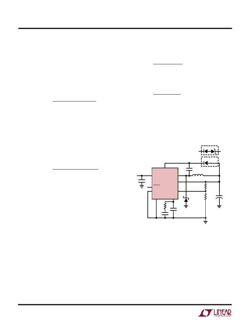
�D2� D4�
�D2�
�P� DISS� (� BOOST� )� =�
�V� OUT� ? (I� SW� / 36) ? V� OUT�
�V� IN�
�V� IN�
�V� IN�
�BOOST�
�LT3431�
�SW�
�C2�
�L1�
�Here� it� can� be� seen� that� Boost� power� dissipation� increases�
�C3�
�BIAS�
�as� the� square� of� Vout.� It� is� possible,� however,� to� reduce�
�V� C2� below� Vout� to� save� power� dissipation� by� increasing�
�the� voltage� drop� in� the� path� of� D2.� Care� should� be� taken�
�SHDN�
�SYNC�
�GND�
�FB�
�V� C�
�D1�
�R1�
�R2�
�+�
�C1�
�that� V� C2� does� not� fall� below� the� minimum� 3.3V� Boost�
�voltage� required� for� full� saturation� of� the� internal� power�
�switch.� For� output� voltages� of� 5V,� V� C2� is� approximately� 5V.�
�During� switch� turn� on,� V� C2� will� fall� as� the� boost� capacitor�
�R� C�
�C� C�
�C� F�
�3431� F09�
�C2� is� dicharged� by� the� boost� pin.� In� a� previous� BOOST� Pin�
�section,� the� value� of� C2� was� designed� for� a� 0.7V� droop� in�
�V� C2� =� V� DROOP� .� Hence,� an� output� voltage� as� low� as� 4V�
�would� still� allow� the� minimum� 3.3V� for� the� boost� function�
�using� the� C2� capacitor� calculated.� If� a� target� output� voltage�
�of� 12V� is� required,� however,� an� excess� of� 8V� is� placed�
�across� the� boost� capacitor� which� is� not� required� for� the�
�boost� function,� but� still� dissipates� additional� power.� What�
�is� required� is� a� voltage� drop� in� the� path� of� D2� to� achieve�
�minimal� power� dissipation� while� still� maintaining� mini-�
�mum� boost� voltage� across� C2.� A� zener,� D4,� placed� in�
�series� with� D2� (see� Figure� 9),� drops� voltage� to� C2.�
�Figure� 9.� BOOST� Pin,� Diode� Selection�
�Input� Voltage� vs� Operating� Frequency� Considerations�
�The� absolute� maximum� input� supply� voltage� for� the� LT3431�
�is� specified� at� 60V.� This� is� based� on� internal� semiconduc-�
�tor� junction� breakdown� effects.� The� practical� maximum�
�input� supply� voltage� for� the� LT3431� may� be� less� than� 60V�
�due� to� internal� power� dissipation� or� switch� minimum� on�
�time� considerations.�
�For� the� extreme� case� of� an� output� short-circuit� fault� to�
�ground,� see� the� section� Short-Circuit� Considerations.�
�sn3431� 3431fs�
�20�
�相关PDF资料 |
PDF描述 |
|---|---|
| MAX6721AUTMSD3+T | IC SUPERVISOR MPU SOT23-6 |
| L06033R9CGWTR | INDUCTOR THIN FILM 3.9NH 0603 |
| LT1076CR | IC REG MULTI CONFIG ADJ 2A D2PAK |
| L06036R8DFWTR | INDUCTOR THIN FILM 6.8NH 0603 |
| LT3972HMSE#PBF | IC REG BUCK ADJ 3.5A 10MSOP |
相关代理商/技术参数 |
参数描述 |
|---|---|
| LT3433 | 制造商:LINER 制造商全称:Linear Technology 功能描述:High Voltage Step-Up/Step-Down DC/DC Converter |
| LT3433_1 | 制造商:LINER 制造商全称:Linear Technology 功能描述:High Voltage Step-Up/Step-Down DC/DC Converter |
| LT3433EFE | 功能描述:IC REG BUCK BST ADJ 0.5A 16TSSOP RoHS:否 类别:集成电路 (IC) >> PMIC - 稳压器 - DC DC 开关稳压器 系列:- 标准包装:2,500 系列:- 类型:降压(降压) 输出类型:固定 输出数:1 输出电压:1.2V,1.5V,1.8V,2.5V 输入电压:2.7 V ~ 20 V PWM 型:- 频率 - 开关:- 电流 - 输出:50mA 同步整流器:是 工作温度:-40°C ~ 125°C 安装类型:表面贴装 封装/外壳:10-TFSOP,10-MSOP(0.118",3.00mm 宽)裸露焊盘 包装:带卷 (TR) 供应商设备封装:10-MSOP 裸露焊盘 |
| LT3433EFE#PBF | 功能描述:IC REG BUCK BST ADJ 0.5A 16TSSOP RoHS:是 类别:集成电路 (IC) >> PMIC - 稳压器 - DC DC 开关稳压器 系列:- 标准包装:250 系列:- 类型:降压(降压) 输出类型:固定 输出数:1 输出电压:1.2V 输入电压:2.05 V ~ 6 V PWM 型:电压模式 频率 - 开关:2MHz 电流 - 输出:500mA 同步整流器:是 工作温度:-40°C ~ 85°C 安装类型:表面贴装 封装/外壳:6-UFDFN 包装:带卷 (TR) 供应商设备封装:6-SON(1.45x1) 产品目录页面:1032 (CN2011-ZH PDF) 其它名称:296-25628-2 |
| LT3433EFE#TR | 功能描述:IC REG BUCK BST ADJ 0.5A 16TSSOP RoHS:否 类别:集成电路 (IC) >> PMIC - 稳压器 - DC DC 开关稳压器 系列:- 标准包装:2,500 系列:- 类型:降压(降压) 输出类型:固定 输出数:1 输出电压:1.2V,1.5V,1.8V,2.5V 输入电压:2.7 V ~ 20 V PWM 型:- 频率 - 开关:- 电流 - 输出:50mA 同步整流器:是 工作温度:-40°C ~ 125°C 安装类型:表面贴装 封装/外壳:10-TFSOP,10-MSOP(0.118",3.00mm 宽)裸露焊盘 包装:带卷 (TR) 供应商设备封装:10-MSOP 裸露焊盘 |
发布紧急采购,3分钟左右您将得到回复。