- 您现在的位置:买卖IC网 > PDF目录14172 > LT3461ES6#TR (Linear Technology)IC REG BOOST ADJ 0.25A TSOT23-6 PDF资料下载
参数资料
| 型号: | LT3461ES6#TR |
| 厂商: | Linear Technology |
| 文件页数: | 4/8页 |
| 文件大小: | 0K |
| 描述: | IC REG BOOST ADJ 0.25A TSOT23-6 |
| 标准包装: | 2,500 |
| 类型: | 升压(升压) |
| 输出类型: | 可调式 |
| 输出数: | 1 |
| 输出电压: | 1.26 V ~ 38 V |
| 输入电压: | 2.5 V ~ 16 V |
| PWM 型: | 电流模式 |
| 频率 - 开关: | 1.3MHz |
| 电流 - 输出: | 250mA |
| 同步整流器: | 无 |
| 工作温度: | -40°C ~ 85°C |
| 安装类型: | 表面贴装 |
| 封装/外壳: | SOT-23-6 细型,TSOT-23-6 |
| 包装: | 带卷 (TR) |
| 供应商设备封装: | TSOT-23-6 |
�� �
�
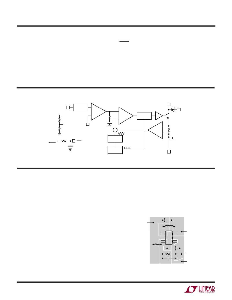
�LT3461/LT3461A�
�PI� FU� CTIO� S�
�SW� (Pin� 1):� Switch� Pin.� Connect� inductor� here.� Minimize�
�trace� at� this� pin� to� reduce� EMI.�
�GND� (Pin� 2):� Ground� Pin.� Tie� directly� to� local� ground�
�plane.�
�FB� (Pin� 3):� Feedback� Pin.� Reference� voltage� is� 1.255V.�
�Connect� resistor� divider� tap� here.� Minimize� trace� area� at�
�FB.� Set� V� OUT� according� to� V� OUT� =� 1.255V� (1� +� R1/R2).�
�BLOCK� DIAGRA�
�SHDN� (Pin� 4):� Shutdown� Pin.� Tie� to� 1.5V� or� higher� to�
�enable� device;� 0.4V� or� less� to� disable� device.� Also� func-�
�tions� as� soft-start.� Use� RC� filter� (47k,� 47nF� typ)� as� shown�
�in� Figure� 1.�
�V� OUT� (Pin� 5):� Output� Pin.� Connect� to� resistor� divider.� Put�
�capacitor� close� to� pin� and� close� to� GND� plane.�
�V� IN� (Pin� 6):� Input� Supply� Pin.� Must� be� locally� bypassed.�
�V� IN� 6�
�V� OUT�
�R1� (EXTERNAL)�
�1.255V�
�REFERENCE�
�+�
�–�
�A1�
�R� C�
�COMPARATOR�
�–�
�A2�
�+�
�R�
�S�
�Q�
�DRIVER�
�1�
�Q1�
�SW�
�5� V� OUT�
�FB�
�R2� (EXTERNAL)�
�3� FB�
�C� C�
�∑�
�+�
�0.1� ?�
�–�
�SHUTDOWN�
�R� S� (EXTERNAL)�
�4� SHDN�
�RAMP�
�GENERATOR�
�C� S� (EXTERNAL)�
�3MHz*�
�R� S� ,� C� S� OPTIONAL� SOFT-START� COMPONENTS�
�OSCILLATOR�
�*LT3461� IS� 1.3MHz�
�2�
�GND�
�3461a� F02�
�Figure� 1.� Block� Diagram�
�OPERATIO�
�The� LT3461/LT3461A� uses� a� constant� frequency,� current�
�mode� control� scheme� to� provide� excellent� line� and� load�
�regulation.� Operation� can� be� best� understood� by� referring�
�to� the� block� diagram� in� Figure� 1.� At� the� start� of� each�
�oscillator� cycle,� the� SR� latch� is� set,� which� turns� on� the�
�power� switch� Q1.� A� voltage� proportional� to� the� switch�
�current� is� added� to� a� stabilizing� ramp� and� the� resulting�
�Layout� Hints�
�The� high� speed� operation� of� the� LT3461/LT3461A� de-�
�mands� careful� attention� to� board� layout.� You� will� not� get�
�advertised� performance� with� careless� layout.� Figure� 2�
�shows� the� recommended� component� placement.�
�C1�
�sum� is� fed� into� the� positive� terminal� of� the� PWM� compara-�
�tor� A2.� When� this� voltage� exceeds� the� level� at� the� negative�
�input� of� A2,� the� SR� latch� is� reset� turning� off� the� power�
�switch.� The� level� at� the� negative� input� of� A2� is� set� by� the�
�error� amplifier� A1,� and� is� simply� an� amplified� version� of�
�GND�
�R2�
�L1�
�V� IN�
�the� difference� between� the� feedback� voltage� and� the�
�reference� voltage� of� 1.255V.� In� this� manner,� the� error�
�amplifier sets the correct peak current level to keep the�
�output� in� regulation.� If� the� error� amplifier’s� output� in-�
�R1�
�C3�
�C2�
�3461a� F03�
�V� OUT�
�SHUTDOWN�
�creases,� more� current� is� delivered� to� the� output;� if� it�
�Figure� 2.� Suggested� Layout�
�decreases,� less� current� is� delivered.�
�3461af�
�4�
�相关PDF资料 |
PDF描述 |
|---|---|
| LT3461AES6#TRM | IC REG BOOST ADJ 0.25A TSOT23-6 |
| LT3461ES6#TRM | IC REG BOOST ADJ 0.25A TSOT23-6 |
| RCC18DREH-S93 | CONN EDGECARD 36POS .100 EYELET |
| ABC19DRTN-S13 | CONN EDGECARD 38POS .100 EXTEND |
| MAX6866UK27D4S+T | IC MPU SUPERVISOR SOT23-5 |
相关代理商/技术参数 |
参数描述 |
|---|---|
| LT3461ES6TRMPBF | 制造商:Linear Technology 功能描述:DC-DC Converter Step-Up 2.5-16V TSOT23-6 |
| LT3462 | 制造商:LINER 制造商全称:Linear Technology 功能描述:Inverting 1.2MHz/2.7MHz DC/DC Converters with Integrated Schottky in ThinSOT |
| LT3462A | 制造商:LINER 制造商全称:Linear Technology 功能描述:Inverting 1.2MHz/2.7MHz DC/DC Converters with Integrated Schottky in ThinSOT |
| LT3462AES6 | 制造商:Linear Technology 功能描述:Conv DC-DC Single Inv 2.5V to 16V 6-Pin TSOT-23 制造商:Linear Technology 功能描述:0.42 A SWITCHING REGULATOR, 3500 kHz SWITCHING FREQ-MAX, PDSO6 |
| LT3462AES6#PBF | 制造商:Linear Technology 功能描述:DC-DC CONVERTER, INVERTING, ADJ, 2.7MHZ, TSOT-23-6, Primary Input Voltage:16V, No. of Outputs:1, No. of Pins:6, Operating Temperature Min:-40C, Operating Temperature Max:85C, MSL:MSL 1 - Unlimited, Package / Case:6-TSOT-23 , RoHS Compliant: Yes 制造商:Linear Technology 功能描述:SP-SWREG/Monolithic, Cut Tape 300mA, Inverting 2.7MHz DC/DC Converter |
发布紧急采购,3分钟左右您将得到回复。