- 您现在的位置:买卖IC网 > PDF目录44984 > LT3468ES5-2#PBF (LINEAR TECHNOLOGY CORP) SPECIALTY ANALOG CIRCUIT, PDSO5 PDF资料下载
参数资料
| 型号: | LT3468ES5-2#PBF |
| 厂商: | LINEAR TECHNOLOGY CORP |
| 元件分类: | 模拟信号调理 |
| 英文描述: | SPECIALTY ANALOG CIRCUIT, PDSO5 |
| 封装: | PLASTIC, SOT-23, MO-193, 5 PIN |
| 文件页数: | 10/12页 |
| 文件大小: | 591K |
| 代理商: | LT3468ES5-2#PBF |
LT3468/LT3468-1/LT3468-2
7
346812f
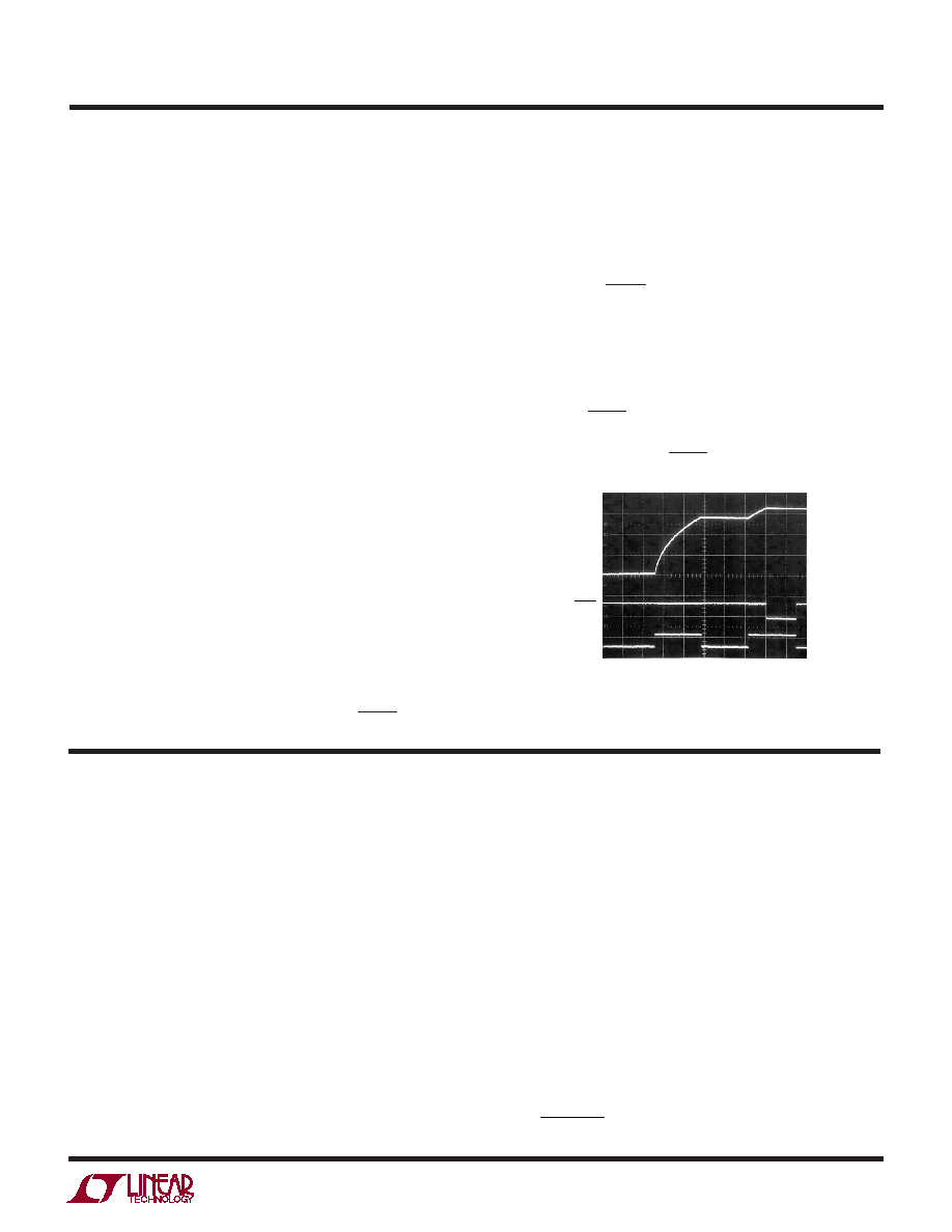
indicating that the part has finished charging. Power
delivery can only be restarted by toggling the CHARGE pin.
The CHARGE pin gives full control of the part to the user.
The charging can be halted at any time by bringing the
CHARGE pin low. Only when the final output voltage is
reached will the DONE pin go low. Figure 2 shows these
various modes in action. When CHARGE is first brought
high, charging commences. When CHARGE is brought
low during charging, the part goes into shutdown and
VOUT no longer rises. When CHARGE is brought high
again, charging resumes. When the target VOUT voltage is
reached, the DONE pin goes low and charging stops.
Finally the CHARGE pin is brought low again so the part
enters shutdown and the DONE pin goes high.
OPERATIO
U
The LT3468/LT3468-1/LT3468-2 are designed to charge
photoflash capacitors quickly and efficiently. The opera-
tion of the part can be best understood by referring to
Figure 1. When the CHARGE pin is first driven high, a one
shot sets both SR latches in the correct state. The power
NPN device, Q1, turns on and current begins ramping up
in the primary of transformer T1. Comparator A1 monitors
the switch current and when the peak current reaches 1.4A
(LT3468), 1A(LT3468-2) or 0.7A (LT3468-1), Q1 is turned
off. Since T1 is utilized as a flyback transformer, the
flyback pulse on the SW pin will cause the output of A3 to
be high. The voltage on the SW pin needs to be at least
36mV higher than VIN for this to happen.
During this phase, current is delivered to the photoflash
capacitor via the secondary and diode D1. As the second-
ary current decreases to zero, the SW pin voltage will begin
to collapse. When the SW pin voltage drops to 36mV
above VIN or lower, the output of A3 (DCM Comparator)
will go low. This fires a one shot which turns Q1 back on.
This cycle will continue to deliver power to the output.
Output voltage detection is accomplished via R2, R1, Q2,
and comparator A2 (VOUT Comparator). Resistors R1 and
R2 are sized so that when the SW voltage is 31.5V above
VIN, the output of A2 goes high which resets the master
latch. This disables Q1 and halts power delivery. NPN
transistor Q3 is turned on pulling the DONE pin low,
LT3468-2
VIN = 3.6V
COUT = 50F
VOUT
100V/DIV
VCHARGE
5V/DIV
VDONE
5V/DIV
1s/DIV
3468 F02
Figure 2. Halting the Charging Cycle with the CHARGE Pin.
APPLICATIO S I FOR ATIO
WU
U
Choosing The Right Device (LT3468/LT3468-1/
LT3468-2)
The only difference between the three versions of the
LT3468 is the peak current level. For the fastest possible
charge time, use the LT3468. The LT3468-1 has the lowest
peak current capability, and is designed for applications
that need a more limited drain on the batteries. Due to the
lower peak current, the LT3468-1 can use a physically
smaller transformer. The LT3468-2 has a current limit in
between that of the LT3468 and the LT3468-1.
Transformer Design
The flyback transformer is a key element for any LT3468/
LT3468-1/LT3468-2 design. It must be designed carefully
and checked that it does not cause excessive current or
voltage on any pin of the part. The main parameters that
need to be designed are shown in Table 1.
The first transformer parameter that needs to be set is the
turns ratio N. The LT3468/LT3468-1/LT3468-2 accom-
plish output voltage detection by monitoring the flyback
waveform on the SW pin. When the SW voltage reaches
31.5V higher than the VIN voltage, the part will halt power
delivery. Thus, the choice of N sets the target output
voltage as it changes the amplitude of the reflected voltage
from the output to the SW pin. Choose N according to the
following equation:
N
VOUT
=
+ 2
31 5
.
相关PDF资料 |
PDF描述 |
|---|---|
| LT3468ES5#PBF | SPECIALTY ANALOG CIRCUIT, PDSO5 |
| LT3470AIDDB#PBF | 0.56 A SWITCHING REGULATOR, PDSO8 |
| LT3470HDDB#TR | 0.2 A SWITCHING REGULATOR, PDSO8 |
| LT3485EDD-0#TRPBF | SPECIALTY ANALOG CIRCUIT, PDSO10 |
| LT3485EDD-0#TR | SPECIALTY ANALOG CIRCUIT, PDSO10 |
相关代理商/技术参数 |
参数描述 |
|---|---|
| LT3469 | 制造商:LINER 制造商全称:Linear Technology 功能描述:Piezo Microactuator Driver with Boost Regulator |
| LT3469ETS8 | 制造商:Linear Technology 功能描述:Piezo Microactuator Driver 8-Pin TSOT-23 |
| LT3469ETS8#PBF | 制造商:Linear Technology 功能描述:SP-Other, CUT TAPE Piezo Microactuator Driver |
| LT3469ETS8#TR | 功能描述:IC AMP DVR W/REG 1.3MHZ TSOT23-8 RoHS:否 类别:集成电路 (IC) >> 线性 - 音頻放大器 系列:- 产品培训模块:Lead (SnPb) Finish for COTS Obsolescence Mitigation Program 标准包装:2,500 系列:DirectDrive® 类型:D 类 输出类型:1-通道(单声道),带立体声耳机 在某负载时最大输出功率 x 通道数量:930mW x 1 @ 8 欧姆; 40mW x 2 @ 16 欧姆 电源电压:2.7 V ~ 5.5 V 特点:消除爆音,差分输入,I²C,静音,关闭,音量控制 安装类型:表面贴装 供应商设备封装:25-WLP(2.09x2.09) 封装/外壳:25-WFBGA,WLCSP 包装:带卷 (TR) 其它名称:MAX97000EWA+T-ND |
| LT3469ETS8#TRM | 功能描述:IC AMP DVR W/REG 1.3MHZ TSOT23-8 RoHS:否 类别:集成电路 (IC) >> 线性 - 音頻放大器 系列:- 产品培训模块:Lead (SnPb) Finish for COTS Obsolescence Mitigation Program 标准包装:2,500 系列:DirectDrive® 类型:D 类 输出类型:1-通道(单声道),带立体声耳机 在某负载时最大输出功率 x 通道数量:930mW x 1 @ 8 欧姆; 40mW x 2 @ 16 欧姆 电源电压:2.7 V ~ 5.5 V 特点:消除爆音,差分输入,I²C,静音,关闭,音量控制 安装类型:表面贴装 供应商设备封装:25-WLP(2.09x2.09) 封装/外壳:25-WFBGA,WLCSP 包装:带卷 (TR) 其它名称:MAX97000EWA+T-ND |
发布紧急采购,3分钟左右您将得到回复。