- 您现在的位置:买卖IC网 > PDF目录44984 > LT3493EDCB-3#TR (LINEAR TECHNOLOGY CORP) 2.2 A SWITCHING REGULATOR, 815 kHz SWITCHING FREQ-MAX, PDSO6 PDF资料下载
参数资料
| 型号: | LT3493EDCB-3#TR |
| 厂商: | LINEAR TECHNOLOGY CORP |
| 元件分类: | 稳压器 |
| 英文描述: | 2.2 A SWITCHING REGULATOR, 815 kHz SWITCHING FREQ-MAX, PDSO6 |
| 封装: | 2 X 3 MM, PLASTIC, MO-229, DFN-6 |
| 文件页数: | 8/20页 |
| 文件大小: | 401K |
| 代理商: | LT3493EDCB-3#TR |
16
LT3493-3
3493-3f
APPLICATIO S I FOR ATIO
WU
U
response. Large electrolytic capacitors may have an ESR
large enough to create an additional zero, and the phase
lead may not be necessary.
If the output capacitor is different than the recommended
capacitor, stability should be checked across all operating
conditions, including load current, input voltage and tem-
perature. The LT1375 data sheet contains a more thor-
ough discussion of loop compensation and describes how
to test the stability using a transient load.
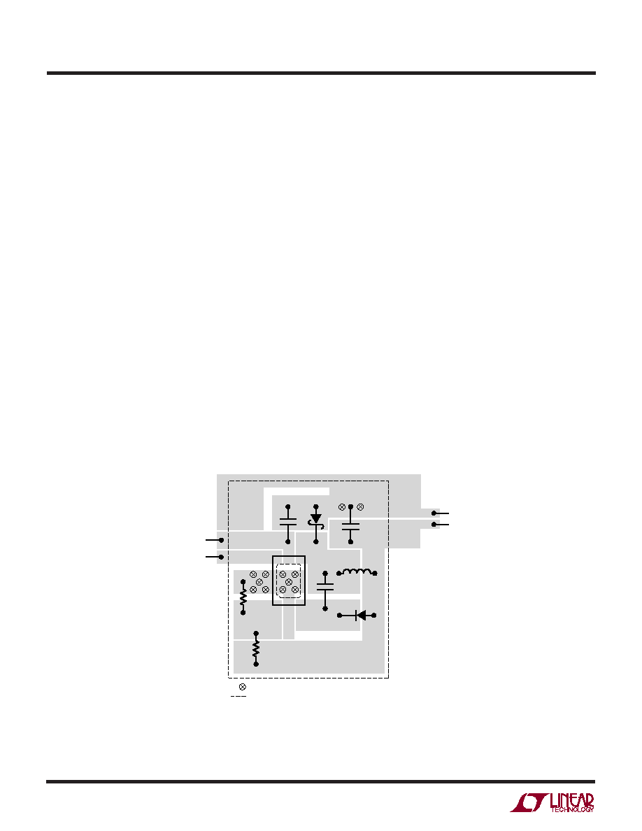
PCB Layout
For proper operation and minimum EMI, care must be
taken during printed circuit board layout. Figure 11 shows
the recommended component placement with trace,
ground plane and via locations. Note that large, switched
currents flow in the LT3493-3’s VIN and SW pins, the catch
diode (D1) and the input capacitor (C2). The loop formed
by these components should be as small as possible and
tied to system ground in only one place. These compo-
nents, along with the inductor and output capacitor,
should be placed on the same side of the circuit board, and
their connections should be made on that layer. Place a
local, unbroken ground plane below these components,
and tie this ground plane to system ground at one location,
ideally at the ground terminal of the output capacitor C1.
The SW and BOOST nodes should be as small as possible.
Finally, keep the FB node small so that the ground pin and
ground traces will shield it from the SW and BOOST nodes.
Include vias near the exposed GND pad of the LT3493-3 to
help remove heat from the LT3493-3 to the ground plane.
High Temperature Considerations
The die temperature of the LT3493-3 must be lower than
the maximum rating of 125
°C. This is generally not a
concern unless the ambient temperature is above 85
°C.
For higher temperatures, care should be taken in the
layout of the circuit to ensure good heat sinking of the
LT3493-3. The maximum load current should be derated
as the ambient temperature approaches 125
°C. The die
temperature is calculated by multiplying the LT3493-3
power dissipation by the thermal resistance from junction
to ambient. Power dissipation within the LT3493-3 can be
estimated by calculating the total power loss from an
efficiency measurement and subtracting the catch diode
C2
D1
C1
SYSTEM
GROUND
: VIAS TO LOCAL GROUND PLANE
: OUTLINE OF LOCAL GROUND PLANE
VOUT
3493-3 F11
VIN
SHUTDOWN
Figure 10. A Good PCB Layout Ensures Proper, Low EMI Operation
相关PDF资料 |
PDF描述 |
|---|---|
| LT3494EDDB#PBF | 0.25 A SWITCHING REGULATOR, PDSO8 |
| LT3494EDDB | 0.25 A SWITCHING REGULATOR, PDSO8 |
| LT3502AEDC#PBF | 1.1 A SWITCHING REGULATOR, 2800 kHz SWITCHING FREQ-MAX, PDSO8 |
| LT3502AIDC#PBF | 1.1 A SWITCHING REGULATOR, 2800 kHz SWITCHING FREQ-MAX, PDSO8 |
| LT3502AIDC#TR | 1.1 A SWITCHING REGULATOR, 2800 kHz SWITCHING FREQ-MAX, PDSO10 |
相关代理商/技术参数 |
参数描述 |
|---|---|
| LT3493EDCBPBF | 制造商:LT 功能描述:Pb Free |
| LT3493EDCB-PBF | 制造商:LINER 制造商全称:Linear Technology 功能描述:1.2A, 750kHz Step-Down Switching Regulator in 2mm × 3mm DFN |
| LT3493EDCB-TR | 制造商:LINER 制造商全称:Linear Technology 功能描述:1.2A, 750kHz Step-Down Switching Regulator in 2mm × 3mm DFN |
| LT3493EDCBTRMPBF | 制造商:Linear Technology 功能描述:Sw. Regulator 1.2A 750kHz Step-Down DFN6 |
| LT3493EDCB-TRPBF | 制造商:LINER 制造商全称:Linear Technology 功能描述:1.2A, 750kHz Step-Down Switching Regulator in 2mm × 3mm DFN |
发布紧急采购,3分钟左右您将得到回复。