- 您现在的位置:买卖IC网 > PDF目录14888 > LT3494EDDB#TRMPBF (Linear Technology)IC REG BOOST ADJ 0.18A 8DFN PDF资料下载
参数资料
| 型号: | LT3494EDDB#TRMPBF |
| 厂商: | Linear Technology |
| 文件页数: | 9/12页 |
| 文件大小: | 0K |
| 描述: | IC REG BOOST ADJ 0.18A 8DFN |
| 标准包装: | 1 |
| 类型: | 升压(升压) |
| 输出类型: | 可调式 |
| 输出数: | 1 |
| 输出电压: | 1.23 V ~ 38 V |
| 输入电压: | 2.3 V ~ 16 V |
| PWM 型: | 混合物 |
| 电流 - 输出: | 180mA |
| 同步整流器: | 无 |
| 工作温度: | -40°C ~ 85°C |
| 安装类型: | 表面贴装 |
| 封装/外壳: | 8-WFDFN 裸露焊盘 |
| 包装: | 标准包装 |
| 供应商设备封装: | 8-DFN(3x2) |
| 产品目录页面: | 1331 (CN2011-ZH PDF) |
| 其它名称: | LT3494EDDB#TRMPBFDKR |
�� �
�
�LT3494/LT3494A�
�APPLICATIONS� INFORMATION�
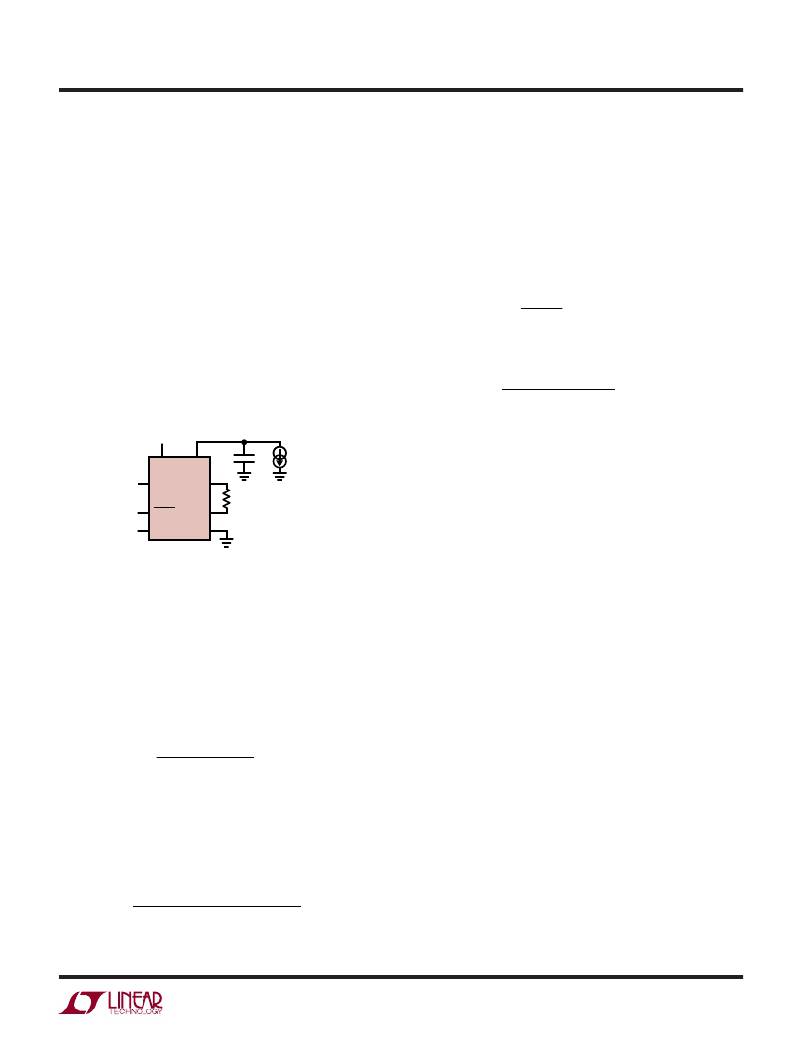
�Connecting� the� Load� to� the� CAP� Node�
�The� ef?ciency� of� the� converter� can� be� improved� by� con-�
�necting� the� load� to� the� CAP� pin� instead� of� the� V� OUT� pin.�
�The� power� loss� in� the� PMOS� disconnect� circuit� is� then�
�made� negligible.� By� connecting� the� feedback� resistor� to�
�the� V� OUT� pin,� no� quiescent� current� will� be� consumed� in� the�
�feedback� resistor� string� during� shutdown� since� the� PMOS�
�If� the� inductor� ripple� current� is� greater� than� the� peak� cur-�
�rent,� then� the� circuit� will� only� operate� in� discontinuous�
�conduction� mode.� The� inductor� value� should� be� increased�
�so� that� I� RIPPLE� <� I� PK� .� An� application� circuit� can� be� designed�
�to� operate� only� in� discontinuous� mode,� but� the� output�
�current� capability� will� be� reduced.�
�Step� 3:� Calculate� the� average� input� current:�
�transistor� will� be� open� (see� Figure� 3).� The� disadvantage�
�of� this� method� is� that� the� CAP� node� cannot� go� to� ground�
�during� shutdown,� but� will� be� limited� to� around� a� diode�
�I� IN� (� AVG� )� =� I� PK� –�
�I� RIPPLE�
�2�
�amps�
�drop� below� V� CC� .� Loads� connected� to� the� part� should� only�
�sink� current.� Never� force� external� power� supplies� onto�
�Step� 4:� Calculate� the� nominal� output� current:�
�I� OUT� (� NOM� )� =�
�the CAP or V� OUT� pins.� The larger value output capacitor�
�(2.2μF� to� 10μF)� should� be� placed� on� the� node� to� which�
�the� load� is� connected.�
�I� IN� (� AVG� )� ?� V� IN� ?� 0� .� 75�
�V� OUT�
�Step� 5:� Derate� output� current:�
�amps�
�1�
�SW�
�8�
�CAP�
�C1�
�I� LOAD�
�I� OUT� =� I� OUT(NOM)� ?� 0.7� amps�
�3�
�V� CC�
�V� OUT�
�7�
�For� low� output� voltages� the� output� current� capability� will�
�5�
�4�
�LT3494�
�SHDN� FB�
�CTRL� GND�
�6�
�2�
�3494� F03�
�be� increased.� When� using� output� disconnect� (load� cur-�
�rent� taken� from� V� OUT� ),� these� higher� currents� will� cause�
�the� drop� in� the� PMOS� switch� to� be� higher� resulting� in�
�reduced� output� current� capability� than� those� predicted�
�V� IN� ?� 400� ?� 10� –� 9�
�I� PK� =� I� LIMIT� +� amps�
�(� V� OUT� +� 1� –� V� IN� )� ?� 150� ?� 10� –� 9�
�I� RIPPLE� =� amps�
�Figure 3. Improved Ef?ciency�
�Maximum� Output� Load� Current�
�The� maximum� output� current� of� a� particular� LT3494/�
�LT3494A� circuit� is� a� function� of� several� circuit� variables.�
�The� following� method� can� be� helpful� in� predicting� the�
�maximum� load� current� for� a� given� circuit:�
�Step� 1:� Calculate� the� peak� inductor� current:�
�L�
�where� I� LIMIT� is� 0.180A� and� 0.350A� for� the� LT3494� and�
�LT3494A� respectively.� L� is� the� inductance� value� in� Henrys�
�and� V� IN� is� the� input� voltage� to� the� boost� circuit.�
�Step� 2:� Calculate� the� inductor� ripple� current:�
�L�
�where� V� OUT� is� the� desired� output� voltage.�
�by� the� preceding� equations.�
�Inrush� Current�
�When� V� CC� is� stepped� from� ground� to� the� operating� volt-�
�age� while� the� output� capacitor� is� discharged,� a� higher�
�level� of� inrush� current� may� ?ow� through� the� inductor�
�and� integrated� Schottky� diode� into� the� output� capacitor.�
�Conditions� that� increase� inrush� current� include� a� larger�
�more� abrupt� voltage� step� at� V� IN� ,� a� larger� output� capacitor�
�tied� to� the� CAP� pin� and� an� inductor� with� a� low� saturation�
�current.� While� the� internal� diode� is� designed� to� handle�
�such� events,� the� inrush� current� should� not� be� allowed� to�
�exceed� 1A.� For� circuits� that� use� output� capacitor� values�
�within� the� recommended� range� and� have� input� voltages�
�of� less� than� 5V,� inrush� current� remains� low,� posing� no�
�hazard� to� the� device.� In� cases� where� there� are� large� steps�
�at� V� CC� (more� than� 5V)� and/or� a� large� capacitor� is� used�
�at� the� CAP� pin,� inrush� current� should� be� measured� to�
�ensure� safe� operation.� The� LT3494A� circuits� experience�
�higher� levels� of� current� during� start-up� and� steady-state�
�operation.� An� external� diode� placed� from� the� SW� pin� to�
�3494fb�
�9�
�相关PDF资料 |
PDF描述 |
|---|---|
| GCA44DTMS | CONN EDGECARD 88POS R/A .125 SLD |
| MAX6465XR54+T | IC VOLT DETECTOR LP SC70-3 |
| VE-JTY-EW-F4 | CONVERTER MOD DC/DC 3.3V 66W |
| MAX6465XR52+T | IC VOLT DETECTOR LP SC70-3 |
| HCM15DSEF-S13 | CONN EDGECARD 30POS .156 EXTEND |
相关代理商/技术参数 |
参数描述 |
|---|---|
| LT3495 | 制造商:LINER 制造商全称:Linear Technology 功能描述:650mA/350mA Micropower Low Noise Boost Converter with Output Disconnect |
| LT3495-1 | 制造商:LINER 制造商全称:Linear Technology 功能描述:650mA/350mA Micropower Low Noise Boost Converter with Output Disconnect |
| LT3495B | 制造商:LINER 制造商全称:Linear Technology 功能描述:650mA/350mA Micropower Low Noise Boost Converter with Output Disconnect |
| LT3495B-1 | 制造商:LINER 制造商全称:Linear Technology 功能描述:650mA/350mA Micropower Low Noise Boost Converter with Output Disconnect |
| LT3495BEDDB#TRMPBF | 功能描述:IC REG BOOST ADJ 0.65A 10DFN RoHS:是 类别:集成电路 (IC) >> PMIC - 稳压器 - DC DC 开关稳压器 系列:- 标准包装:2,500 系列:- 类型:升压(升压) 输出类型:可调式 输出数:1 输出电压:1.24 V ~ 30 V 输入电压:1.5 V ~ 12 V PWM 型:电流模式,混合 频率 - 开关:600kHz 电流 - 输出:500mA 同步整流器:无 工作温度:-40°C ~ 85°C 安装类型:表面贴装 封装/外壳:8-SOIC(0.154",3.90mm 宽) 包装:带卷 (TR) 供应商设备封装:8-SOIC |
发布紧急采购,3分钟左右您将得到回复。