- 您现在的位置:买卖IC网 > PDF目录44984 > LT3494EDDB (LINEAR TECHNOLOGY CORP) 0.25 A SWITCHING REGULATOR, PDSO8 PDF资料下载
参数资料
| 型号: | LT3494EDDB |
| 厂商: | LINEAR TECHNOLOGY CORP |
| 元件分类: | 稳压器 |
| 英文描述: | 0.25 A SWITCHING REGULATOR, PDSO8 |
| 封装: | 3 X 2 MM, PLASTIC, MO-229WECD-1, DFN-8 |
| 文件页数: | 12/12页 |
| 文件大小: | 261K |
| 代理商: | LT3494EDDB |
LT3494/LT3494A
9
3494fb
APPLICATIONS INFORMATION
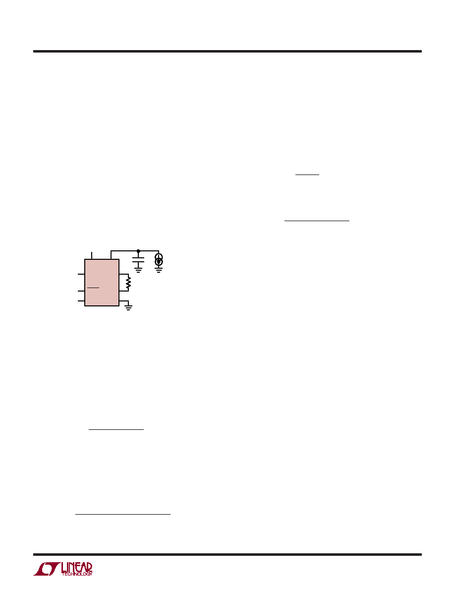
Connecting the Load to the CAP Node
The efciency of the converter can be improved by con-
necting the load to the CAP pin instead of the VOUT pin.
The power loss in the PMOS disconnect circuit is then
made negligible. By connecting the feedback resistor to
the VOUT pin, no quiescent current will be consumed in the
feedback resistor string during shutdown since the PMOS
transistor will be open (see Figure 3). The disadvantage
of this method is that the CAP node cannot go to ground
during shutdown, but will be limited to around a diode
drop below VCC. Loads connected to the part should only
sink current. Never force external power supplies onto
the CAP or VOUT pins. The larger value output capacitor
(2.2μF to 10μF) should be placed on the node to which
the load is connected.
Figure 3. Improved Efciency
Maximum Output Load Current
The maximum output current of a particular LT3494/
LT3494A circuit is a function of several circuit variables.
The following method can be helpful in predicting the
maximum load current for a given circuit:
Step 1: Calculate the peak inductor current:
II
V
L
amps
PK
LIMIT
IN
=+
–
400 10
9
where ILIMIT is 0.180A and 0.350A for the LT3494 and
LT3494A respectively. L is the inductance value in Henrys
and VIN is the input voltage to the boost circuit.
Step 2: Calculate the inductor ripple current:
I
VV
L
amps
RIPPLE
OUT
IN
=
+
()
1
150 10
9
–
–
where VOUT is the desired output voltage.
If the inductor ripple current is greater than the peak cur-
rent, then the circuit will only operate in discontinuous
conduction mode. The inductor value should be increased
so that IRIPPLE < IPK. An application circuit can be designed
to operate only in discontinuous mode, but the output
current capability will be reduced.
Step 3: Calculate the average input current:
II
I
amps
IN AVG
PK
RIPPLE
()
–
=
2
Step 4: Calculate the nominal output current:
I
IV
V
amps
OUT NOM
IN AVG
IN
OUT
()
() .
=
075
Step 5: Derate output current:
IOUT = IOUT(NOM) 0.7 amps
For low output voltages the output current capability will
be increased. When using output disconnect (load cur-
rent taken from VOUT), these higher currents will cause
the drop in the PMOS switch to be higher resulting in
reduced output current capability than those predicted
by the preceding equations.
Inrush Current
When VCC is stepped from ground to the operating volt-
age while the output capacitor is discharged, a higher
level of inrush current may ow through the inductor
and integrated Schottky diode into the output capacitor.
Conditions that increase inrush current include a larger
more abrupt voltage step at VIN, a larger output capacitor
tied to the CAP pin and an inductor with a low saturation
current. While the internal diode is designed to handle
such events, the inrush current should not be allowed to
exceed 1A. For circuits that use output capacitor values
within the recommended range and have input voltages
of less than 5V, inrush current remains low, posing no
hazard to the device. In cases where there are large steps
at VCC (more than 5V) and/or a large capacitor is used
at the CAP pin, inrush current should be measured to
ensure safe operation. The LT3494A circuits experience
higher levels of current during start-up and steady-state
operation. An external diode placed from the SW pin to
SW
CAP
VCC
SHDN
CTRL
VOUT
FB
GND
3
5
4
7
6
2
3494 F03
LT3494
C1
ILOAD
18
相关PDF资料 |
PDF描述 |
|---|---|
| LT3502AEDC#PBF | 1.1 A SWITCHING REGULATOR, 2800 kHz SWITCHING FREQ-MAX, PDSO8 |
| LT3502AIDC#PBF | 1.1 A SWITCHING REGULATOR, 2800 kHz SWITCHING FREQ-MAX, PDSO8 |
| LT3502AIDC#TR | 1.1 A SWITCHING REGULATOR, 2800 kHz SWITCHING FREQ-MAX, PDSO10 |
| LT3502AEDC#TRM | 1.1 A SWITCHING REGULATOR, 2800 kHz SWITCHING FREQ-MAX, PDSO10 |
| LT3502IDC#TR | 1.1 A SWITCHING REGULATOR, 1400 kHz SWITCHING FREQ-MAX, PDSO10 |
相关代理商/技术参数 |
参数描述 |
|---|---|
| LT3494EDDB#PBF | 制造商:Linear Technology 功能描述:DC-DC CONVERTER BOOST DFN-8 制造商:Linear Technology 功能描述:DC-DC CONVERTER, BOOST, DFN-8; Primary Input Voltage:16V; No. of Outputs:1; Output Current:180mA; No. of Pins:8; Operating Temperature Min:-40C; Operating Temperature Max:85C; Package / Case:8-DFN; Supply Voltage Max:16V ;RoHS Compliant: Yes |
| LT3494EDDB#TRM | 制造商:Linear Technology 功能描述:MICROPOWER LOW NOISE BOOST CONVERTERS WITH OUTPUT DISCONNECT |
| LT3494EDDB#TRMPBF | 功能描述:IC REG BOOST ADJ 0.18A 8DFN RoHS:是 类别:集成电路 (IC) >> PMIC - 稳压器 - DC DC 开关稳压器 系列:- 产品培训模块:High Efficiency Current Mode Switching Regulators CMOS LDO Regulators 特色产品:BD91x Series Step-Down Regulators 标准包装:2,500 系列:- 类型:降压(降压) 输出类型:两者兼有 输出数:2 输出电压:3.3V,0.8 V ~ 2.5 V 输入电压:4.5 V ~ 5.5 V PWM 型:电流模式 频率 - 开关:1MHz 电流 - 输出:1.5A 同步整流器:是 工作温度:-40°C ~ 85°C 安装类型:表面贴装 封装/外壳:20-VFQFN 裸露焊盘 包装:带卷 (TR) 供应商设备封装:VQFN020V4040 产品目录页面:1373 (CN2011-ZH PDF) 其它名称:BD9152MUV-E2TR |
| LT3494EDDB#TRPBF | 功能描述:IC REG BOOST ADJ 0.18A 8DFN RoHS:是 类别:集成电路 (IC) >> PMIC - 稳压器 - DC DC 开关稳压器 系列:- 标准包装:500 系列:- 类型:切换式电容器(充电泵),反相 输出类型:固定 输出数:1 输出电压:-3V 输入电压:2.3 V ~ 5.5 V PWM 型:Burst Mode? 频率 - 开关:900kHz 电流 - 输出:100mA 同步整流器:无 工作温度:-40°C ~ 85°C 安装类型:表面贴装 封装/外壳:SOT-23-6 细型,TSOT-23-6 包装:带卷 (TR) 供应商设备封装:TSOT-23-6 其它名称:LTC1983ES6-3#TRMTR |
| LT3494EDDBTRMPBF | 制造商:Linear Technology 功能描述:Boost Converter uPower Low Noise DFN8EP |
发布紧急采购,3分钟左右您将得到回复。