- 您现在的位置:买卖IC网 > PDF目录79835 > LT3495BEDDB-1#TRPBF (LINEAR TECHNOLOGY CORP) 0.45 A SWITCHING REGULATOR, PDSO10 PDF资料下载
参数资料
| 型号: | LT3495BEDDB-1#TRPBF |
| 厂商: | LINEAR TECHNOLOGY CORP |
| 元件分类: | 稳压器 |
| 英文描述: | 0.45 A SWITCHING REGULATOR, PDSO10 |
| 封装: | 3 X 2 MM, LEAD FREE, PLASTIC, MO-229WECD-1, DFN-10 |
| 文件页数: | 4/16页 |
| 文件大小: | 299K |
| 代理商: | LT3495BEDDB-1#TRPBF |
LT3495/LT3495B/
LT3495-1/LT3495B-1
12
3495b1b1fa
APPLICATIONS INFORMATION
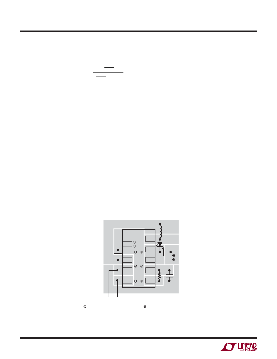
Figure 6. Recommended Board Layout
can be set by the value of RCTRL and CCTRL. The following
expression can be used to design the soft-start time:
TSTART UP =RCTRL CCTRL In
V
SHDN
V
SHDN
– 1.235
where VSHDN is the voltage at SHDN pin when the part is
enabled. To ensure soft-start will work, the initial voltage
at CTRL pin when the part is enabled should be close to
0V. The soft-start may not work if this initial condition is
not satised.
Output Disconnect
The LT3495 series has an output disconnect PMOS that
blocks the load from the input during shutdown. During
normal operation, the maximum current through the PMOS
is limited by circuitry inside the chip. When the CAP and
VOUT voltage difference is more than 8.7V (typ), the cur-
rent through the PMOS is no longer limited, and can be
much higher. As a result, forcing 8.7V or higher voltage
from the CAP to the VOUT pins can damage the PMOS.
In cases when the CAP voltage is high and/or a large ca-
pacitor is used at the CAP pin, shorting VOUT to GND can
cause large PMOS currents to ow. Under this condition,
the PMOS peak current should be kept at less than 1A.
Also be aware of the thermal dissipation in the PMOS at
all times. In addition, if the input voltage is more than 8V,
the PMOS will turn on during shutdown, resulting in the
output voltage no longer being blocked from the input.
Under this condition, the output voltage will be about 8V
lower than the input voltage.
Board Layout Considerations
As with all switching regulators, careful attention must be
paid to the PCB board layout and component placement.
To maximize efciency, switch rise and fall times are made
as short as possible. To prevent electromagnetic interfer-
ence (EMI) problems, proper layout of the high frequency
switching path is essential. The voltage signal of the
SW pin has sharp rising and falling edges. Minimize the
length and area of all traces connected to the SW pin and
always use a ground plane under the switching regulator
to minimize interplane coupling. In addition, the FB pin
feeds into the internal error amplier and is sensitive to
noise. Minimizing the length and area of all traces to this
pin is recommended. Connect the feedback resistor R1
directly from the VOUT pin to the FB pin and keep the trace
as short as possible. Recommended component placement
is shown in Figure 6.
GND
VCC
CTRL
SHDN
SW
CAP
VOUT
FB
GND
CTRL
VIAS TO GROUND PLANE REQUIRED
TO IMPROVE THERMAL PERFORMANCE
VIAS FOR CAP GROUND RETURN THROUGH
SECOND METAL LAYER, CAPACITOR GROUNDS
MUST BE RETURNED DIRECTLY TO IC GROUND
SHDN
3495 F06
GND
相关PDF资料 |
PDF描述 |
|---|---|
| LSN-2.5/10-D12B | 1-OUTPUT DC-DC REG PWR SUPPLY MODULE |
| LSM-5/16-D12 | 1-OUTPUT 80 W DC-DC REG PWR SUPPLY MODULE |
| LM4041CIZADJ | 1-OUTPUT TWO TERM VOLTAGE REFERENCE, 1.233 V, PBCY3 |
| LS4301-9PD7T | 1-OUTPUT 100 W AC-DC PWR FACTOR CORR MODULE |
| LS4301-9PD9TB1 | 1-OUTPUT 100 W AC-DC PWR FACTOR CORR MODULE |
相关代理商/技术参数 |
参数描述 |
|---|---|
| LT3495BEDDB-PBF | 制造商:LINER 制造商全称:Linear Technology 功能描述:650mA/350mA Micropower Low Noise Boost Converter with Output Disconnect |
| LT3495BEDDB-TRPBF | 制造商:LINER 制造商全称:Linear Technology 功能描述:650mA/350mA Micropower Low Noise Boost Converter with Output Disconnect |
| LT3495EDDB#PBF | 制造商:Linear Technology 功能描述:DC-DC CONVERTER BOOST DFN-10 制造商:Linear Technology 功能描述:DC-DC CONVERTER, BOOST, DFN-10 制造商:Linear Technology 功能描述:DC-DC CONVERTER, BOOST, DFN-10, Primary Input Voltage:16V, No. of Outputs:1, No. of Pins:10, Operating Temperature Min:-40C, Operating Temperature Max:125C, MSL:MSL 1 - Unlimited, Package / Case:10-DFN , RoHS Compliant: Yes 制造商:Linear Technology 功能描述:SP-SWREG/Monolithic, Cut Tape Micropower 650mA (|sw) Low Noise Boost Converter w |
| LT3495EDDB#TRMPBF | 功能描述:IC REG BOOST ADJ 0.65A 10DFN RoHS:是 类别:集成电路 (IC) >> PMIC - 稳压器 - DC DC 开关稳压器 系列:- 产品培训模块:High Efficiency Current Mode Switching Regulators CMOS LDO Regulators 特色产品:BD91x Series Step-Down Regulators 标准包装:2,500 系列:- 类型:降压(降压) 输出类型:两者兼有 输出数:2 输出电压:3.3V,0.8 V ~ 2.5 V 输入电压:4.5 V ~ 5.5 V PWM 型:电流模式 频率 - 开关:1MHz 电流 - 输出:1.5A 同步整流器:是 工作温度:-40°C ~ 85°C 安装类型:表面贴装 封装/外壳:20-VFQFN 裸露焊盘 包装:带卷 (TR) 供应商设备封装:VQFN020V4040 产品目录页面:1373 (CN2011-ZH PDF) 其它名称:BD9152MUV-E2TR |
| LT3495EDDB#TRPBF | 功能描述:IC REG BOOST ADJ 0.65A 10DFN RoHS:是 类别:集成电路 (IC) >> PMIC - 稳压器 - DC DC 开关稳压器 系列:- 标准包装:2,500 系列:- 类型:升压(升压) 输出类型:可调式 输出数:1 输出电压:1.24 V ~ 30 V 输入电压:1.5 V ~ 12 V PWM 型:电流模式,混合 频率 - 开关:600kHz 电流 - 输出:500mA 同步整流器:无 工作温度:-40°C ~ 85°C 安装类型:表面贴装 封装/外壳:8-SOIC(0.154",3.90mm 宽) 包装:带卷 (TR) 供应商设备封装:8-SOIC |
发布紧急采购,3分钟左右您将得到回复。