- 您现在的位置:买卖IC网 > PDF目录79692 > LT3500EMSE#PBF (LINEAR TECHNOLOGY CORP) 3.5 A SWITCHING REGULATOR, 2800 kHz SWITCHING FREQ-MAX, PDSO16 PDF资料下载
参数资料
| 型号: | LT3500EMSE#PBF |
| 厂商: | LINEAR TECHNOLOGY CORP |
| 元件分类: | 稳压器 |
| 英文描述: | 3.5 A SWITCHING REGULATOR, 2800 kHz SWITCHING FREQ-MAX, PDSO16 |
| 封装: | LEAD FREE, PLASTIC, MSOP-16 |
| 文件页数: | 23/28页 |
| 文件大小: | 318K |
| 代理商: | LT3500EMSE#PBF |
第1页第2页第3页第4页第5页第6页第7页第8页第9页第10页第11页第12页第13页第14页第15页第16页第17页第18页第19页第20页第21页第22页当前第23页第24页第25页第26页第27页第28页
LT3500
4
3500fc
PARAMETER
CONDITIONS
MIN
TYP
MAX
UNITS
LFB Voltage
VLDRV = VLFB
l
0.784
0.8
0.816
V
LFB Line/Load Regulation
VVIN = 3V to 40V, VLDRV = VLFB
l
0.776
0.8
0.824
V
SS to LFB Offset (VSS – VLFB)VSS = 0.8V, VLDRV = VLFB
90
115
140
mV
LFB Bias Current
VLFB = 0.8V
115
300
nA
LDRV Dropout (VVIN – VLDRV)VLDRV = 3V, ILDRV = 5mA
l
0.8
1.2
1.6
V
LDRV Maximum Current
VLDRV = 0V
l
913
18
mA
ELECTRICAL CHARACTERISTICS The l denotes the specications which apply over the full operating
temperature range, otherwise specications are at TJ = 25°C. VVIN = 15V, VRT/SYNC = 2V, unless otherwise specied.
Note 1: Stresses beyond those listed under Absolute Maximum Ratings
may cause permanent damage to the device. Exposure to any Absolute
Maximum Rating condition for extended periods may affect device
reliability and lifetime.
Note2: The LT3500EDD/LT3500EMSE is guaranteed to meet performance
specications from 0°C to 125°C junction temperature. Specications over
the –40°C to 125°C operating junction temperature range are assured by
design, characterization and correlation with statistical process controls.
The LT3500IDD/LT3500IMSE is guaranteed over the full –40°C to 125°C
operating junction temperature range. The LT3500HDD/LT3500HMSE is
guaranteed over the full –40°C to 150°C operating junction temperature
range. High junction temperatures degrade operating lifetimes. Operating
lifetime is derated at junction temperatures greater than 125°C.
Note 3: Minimum input voltage is dened as the voltage where internal
bias lines are regulated so that the reference voltage and oscillator remain
constant. Actual minimum input voltage to maintain a regulated output
will depend upon output voltage and load current. See Applications
Information.
Note 4: An internal power-on reset (POR) latch is set on the positive
transition of the SHDN pin through its threshold. The output of the latch
activates a current source on the SS pin which typically sinks 600μA,
discharging the SS capacitor. The latch is reset when the SS pin is driven
below the soft-start POR threshold or the SHDN pin is taken below its
threshold.
Note 5: This is the minimum voltage across the boost capacitor needed to
guarantee full saturation of the internal power switch.
Note 6: This IC includes overtemperature protection that is intended
to protect the device during momentary overload conditions. Junction
temperature will exceed the maximum operating junction temperature
when overtemperature protection is active. Continuous operation above
the specied maximum operating junction temperature may impair device
reliability.
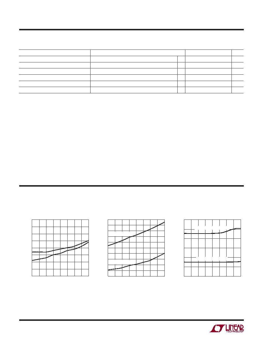
TYPICAL PERFORMANCE CHARACTERISTICS
Feedback Voltage vs Temperature
RT/SYNC Voltage vs Temperature
Shutdown Threshold and Minimum
Input Voltage vs Temperature
TEMPERATURE (°C)
–50
VOL
TAGE
(V)
0.800
FB
LFB
0.810
150
3500 G01
0.790
0.780
0
50
100
–25
25
75
125
0.820
0.795
0.805
0.785
0.815
TEMPERATURE (°C)
–50
0.90
VOLTAGE
(V)
0.92
0.96
0.98
1.00
1.10
1.04
0
50
75
3500 G02
0.94
1.06
1.08
1.02
–25
25
100 125
150
RRT/SYNC = 90.9k
RRT/SYNC = 15k
TEMPERATURE (°C)
–50
VOLTAGE
(V)
2.0
2.5
3.0
25
75
3500 G03
1.5
1.0
–25
0
50
100
150
125
0.5
0
MINIMUM INPUT VOLTAGE
SHUTDOWN THRESHOLD
相关PDF资料 |
PDF描述 |
|---|---|
| LSP3120K50E | SWITCHING REGULATOR, PSSO5 |
| LS1001-7EPD3T | 1-OUTPUT 100 W AC-DC REG PWR SUPPLY MODULE |
| LS1001-7ERD2B1 | 1-OUTPUT 100 W AC-DC REG PWR SUPPLY MODULE |
| LS1001-7PD6B1 | 1-OUTPUT 100 W AC-DC REG PWR SUPPLY MODULE |
| LS1001-9EPD0T | 1-OUTPUT 100 W AC-DC REG PWR SUPPLY MODULE |
相关代理商/技术参数 |
参数描述 |
|---|---|
| LT3500EMSE-TRPBF | 制造商:LINER 制造商全称:Linear Technology 功能描述:Monolithic 2A Step-Down Regulator Plus Linear Regulator/Controller |
| LT3500HDD#PBF | 功能描述:IC REG DL BUCK/LINEAR 12-DFN RoHS:是 类别:集成电路 (IC) >> PMIC - 稳压器 - 线性 + 切换式 系列:- 标准包装:2,500 系列:- 拓扑:降压(降压)同步(3),线性(LDO)(2) 功能:任何功能 输出数:5 频率 - 开关:300kHz 电压/电流 - 输出 1:控制器 电压/电流 - 输出 2:控制器 电压/电流 - 输出 3:控制器 带 LED 驱动器:无 带监控器:无 带序列发生器:是 电源电压:5.6 V ~ 24 V 工作温度:-40°C ~ 85°C 安装类型:* 封装/外壳:* 供应商设备封装:* 包装:* |
| LT3500HDD#TRPBF | 功能描述:IC REG DL BUCK/LINEAR 12-DFN RoHS:是 类别:集成电路 (IC) >> PMIC - 稳压器 - 线性 + 切换式 系列:- 标准包装:2,500 系列:- 拓扑:降压(降压)同步(3),线性(LDO)(2) 功能:任何功能 输出数:5 频率 - 开关:300kHz 电压/电流 - 输出 1:控制器 电压/电流 - 输出 2:控制器 电压/电流 - 输出 3:控制器 带 LED 驱动器:无 带监控器:无 带序列发生器:是 电源电压:5.6 V ~ 24 V 工作温度:-40°C ~ 85°C 安装类型:* 封装/外壳:* 供应商设备封装:* 包装:* |
| LT3500HDD-PBF | 制造商:LINER 制造商全称:Linear Technology 功能描述:Monolithic 2A Step-Down Regulator Plus Linear Regulator/Controller |
| LT3500HDD-TRPBF | 制造商:LINER 制造商全称:Linear Technology 功能描述:Monolithic 2A Step-Down Regulator Plus Linear Regulator/Controller |
发布紧急采购,3分钟左右您将得到回复。