- 您现在的位置:买卖IC网 > PDF目录14095 > LT3502AEMS#TRPBF (Linear Technology)IC REG BUCK ADJ 0.5A 10MSOP PDF资料下载
参数资料
| 型号: | LT3502AEMS#TRPBF |
| 厂商: | Linear Technology |
| 文件页数: | 10/24页 |
| 文件大小: | 0K |
| 描述: | IC REG BUCK ADJ 0.5A 10MSOP |
| 标准包装: | 2,500 |
| 类型: | 降压(降压) |
| 输出类型: | 可调式 |
| 输出数: | 1 |
| 输出电压: | 0.8 V ~ 36 V |
| 输入电压: | 3 V ~ 40 V |
| PWM 型: | 电流模式 |
| 频率 - 开关: | 2.2MHz |
| 电流 - 输出: | 500mA |
| 同步整流器: | 无 |
| 工作温度: | -40°C ~ 125°C |
| 安装类型: | 表面贴装 |
| 封装/外壳: | 10-TFSOP,10-MSOP(0.118",3.00mm 宽) |
| 包装: | 带卷 (TR) |
| 供应商设备封装: | 10-MSOP |
�� �
�
�LT3502/LT3502A�
�APPLICATIONS� INFORMATION�
�R1� =� R2� ?� OUT� –� 1� ?�
�V� OUT� +� V� D�
�V� IN(MIN)� =� OUT�
�–� V� D� +� V� SW�
�1μs/DIV�
�V� OUT� +� V� D�
�DC� MIN�
�FBResistorNetwork�
�The� output� voltage� is� programmed� with� a� resistor� divider�
�between� the� output� and� the� FB� pin.� Choose� the� 1%� resis-�
�tors� according� to:�
�?� V� ?�
�?� 0.8V� ?�
�R2� should� be� 20k� or� less� to� avoid� bias� current� errors.�
�Reference� designators� refer� to� the� Block� Diagram.�
�Input� Voltage� Range�
�The� input� voltage� range� for� the� LT3502/LT3502A� applica-�
�tions� depends� on� the� output� voltage� and� on� the� absolute�
�maximum� ratings� of� the� V� IN� and� BOOST� pins.�
�The� minimum� input� voltage� is� determined� by� either� the�
�LT3502/LT3502A’s� minimum� operating� voltage� of� 3V,� or�
�by� its� maximum� duty� cycle.� The� duty� cycle� is� the� fraction�
�of� time� that� the� internal� switch� is� on� and� is� determined�
�by� the� input� and� output� voltages:�
�DC� =�
�V� IN� –� V� SW� +� V� D�
�where� V� D� is� the� forward� voltage� drop� of� the� catch� diode�
�(~0.4V)� and� V� SW� is� the� voltage� drop� of� the� internal� switch�
�(~0.45V� at� maximum� load).� This� leads� to� a� minimum� input�
�voltage� of:�
�V� +� V� D�
�DC� MAX�
�with� DC� MAX� =� 0.80� for� the� LT3502A� and� 0.90� for� the�
�LT3502.�
�The� maximum� input� voltage� is� determined� by� the�
�absolute� maximum� ratings� of� the� V� IN� and� BOOST� pins.� For�
�fixed� frequency� operation,� the� maximum� input� voltage� is�
�determined� by� the� minimum� duty� cycle� DC� MIN� :�
�V� IN(MAX)� =� –� V� D� +� V� SW�
�DC� MIN� =� 0.15� for� the� LT3502A� and� 0.08� for� the� LT3502.�
�10�
�Note� that� this� is� a� restriction� on� the� operating� input� volt-�
�age� for� fixed� frequency� operation;� the� circuit� will� tolerate�
�transient� inputs� up� to� the� absolute� maximum� ratings� of�
�the� V� IN� and� BOOST� pins.� The� input� voltage� should� be�
�limited� to� the� V� IN� operating� range� (40V)� during� overload�
�conditions.�
�Minimum� On-Time�
�The� LT3502/LT3502A� will� still� regulate� the� output� at� input�
�voltages� that� exceed� V� IN(MAX)� (up� to� 40V),� however,� the�
�output� voltage� ripple� increases� as� the� input� voltage� is�
�increased.�
�As� the� input� voltage� is� increased,� the� part� is� required� to�
�switch� for� shorter� periods� of� time.� Delays� associated� with�
�turning� off� the� power� switch� dictate� the� minimum� on-time�
�of� the� part.� The� minimum� on-time� for� the� LT3502/LT3502A�
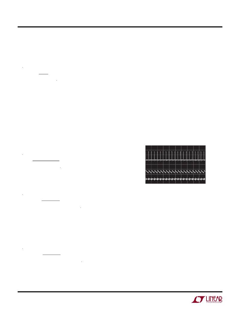
�is� 60ns� (Figure� 1).�
�V� SW�
�20V/DIV�
�I� L�
�500mA/DIV�
�V� OUT�
�100mV/DIV�
�3502� F01�
�V� IN� =� 33V,� V� OUT� =� 3.3V�
�L� =� 6.8μH,� C� OUT� =� 10μF,� I� OUT� =� 250mA�
�Figure� 1.� Continuous� Mode� Operation� Near�
�Minimum� On-Time� of� 60ns�
�When� the� required� on-time� decreases� below� the� mini-�
�mum� on-time� of� 60ns,� instead� of� the� switch� pulse� width�
�becoming� narrower� to� accommodate� the� lower� duty� cycle�
�requirement,� the� switch� pulse� width� remains� fixed� at�
�60ns.� The� inductor� current� ramps� up� to� a� value� exceed-�
�ing� the� load� current� and� the� output� ripple� increases.� The�
�part� then� remains� off� until� the� output� voltage� dips� below�
�the� programmed� value� before� it� begins� switching� again�
�(Figure� 2).�
�Provided� that� the� load� can� tolerate� the� increased� output�
�voltage� ripple� and� that� the� components� have� been� properly�
�selected,� operation� above� V� IN(MAX)� is� safe� and� will� not�
�damage� the� part.�
�3502fd�
�相关PDF资料 |
PDF描述 |
|---|---|
| HM66A-0745101MLF13 | SHIELDED POWER INDUCTORS |
| MAX6868UK31D1S+T | IC MPU SUPERVISOR SOT23-5 |
| ASPI-0310FSSA-6R8M-T4 | INDUCTOR SHLD POWER 6.8UH SMD |
| HM71-101R5LFTR | HIGH PERF LOW COST INDUCTORS |
| MAX6868UK31D5L+T | IC MPU SUPERVISOR SOT23-5 |
相关代理商/技术参数 |
参数描述 |
|---|---|
| LT3502AIDC#PBF | 制造商:Linear Technology 功能描述:Conv DC-DC Single Step Down 3V to 40V 8-Pin DFN EP 制造商:Linear Technology 功能描述:Bulk 制造商:Linear Technology 功能描述:DC-DC CONVERTER BUCK 2.2MHZ 制造商:Linear Technology 功能描述:DC-DC CONVERTER, BUCK, 2.2MHZ, DFN-8; Primary Input Voltage:40V; No. of Outputs:1; Output Current:500mA; No. of Pins:8; Operating Temperature Min:-40C; Operating Temperature Max:125C; Operating Temperature Range:-40C to +125C ;RoHS Compliant: Yes |
| LT3502AIDC#TRMPBF | 功能描述:IC REG BUCK ADJ 0.5A 8DFN RoHS:是 类别:集成电路 (IC) >> PMIC - 稳压器 - DC DC 开关稳压器 系列:- 标准包装:250 系列:- 类型:降压(降压) 输出类型:固定 输出数:1 输出电压:1.2V 输入电压:2.05 V ~ 6 V PWM 型:电压模式 频率 - 开关:2MHz 电流 - 输出:500mA 同步整流器:是 工作温度:-40°C ~ 85°C 安装类型:表面贴装 封装/外壳:6-UFDFN 包装:带卷 (TR) 供应商设备封装:6-SON(1.45x1) 产品目录页面:1032 (CN2011-ZH PDF) 其它名称:296-25628-2 |
| LT3502AIDC#TRPBF | 功能描述:IC REG BUCK ADJ 0.5A 8DFN RoHS:是 类别:集成电路 (IC) >> PMIC - 稳压器 - DC DC 开关稳压器 系列:- 标准包装:2,500 系列:- 类型:升压(升压) 输出类型:可调式 输出数:1 输出电压:1.24 V ~ 30 V 输入电压:1.5 V ~ 12 V PWM 型:电流模式,混合 频率 - 开关:600kHz 电流 - 输出:500mA 同步整流器:无 工作温度:-40°C ~ 85°C 安装类型:表面贴装 封装/外壳:8-SOIC(0.154",3.90mm 宽) 包装:带卷 (TR) 供应商设备封装:8-SOIC |
| LT3502AIDC-PBF | 制造商:LINER 制造商全称:Linear Technology 功能描述:1.1MHz/2.2MHz, 500mA Step-Down Regulators in 2mm × 2mm DFN and MS10 |
| LT3502AIDCTRMPBF | 制造商:Linear Technology 功能描述:DC-DC Converter Step-Down 3-40V DFN8EP |
发布紧急采购,3分钟左右您将得到回复。