- 您现在的位置:买卖IC网 > PDF目录44984 > LT3502AIDC#PBF (LINEAR TECHNOLOGY CORP) 1.1 A SWITCHING REGULATOR, 2800 kHz SWITCHING FREQ-MAX, PDSO8 PDF资料下载
参数资料
| 型号: | LT3502AIDC#PBF |
| 厂商: | LINEAR TECHNOLOGY CORP |
| 元件分类: | 稳压器 |
| 英文描述: | 1.1 A SWITCHING REGULATOR, 2800 kHz SWITCHING FREQ-MAX, PDSO8 |
| 封装: | 2 X 2 MM, LEAD FREE, PLASTIC, DFN-8 |
| 文件页数: | 5/24页 |
| 文件大小: | 386K |
| 代理商: | LT3502AIDC#PBF |
LT3502/LT3502A
13
3502fd
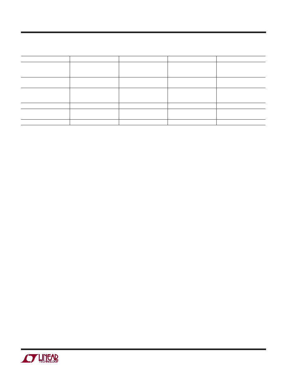
Table 2
VENDOR
PHONE
URL
PART SERIES
COMMENTS
Panasonic
(714) 373-7366
www.panasonic.com
Ceramic
Polymer,
Tantalum
EEF Series
Kemet
(864) 963-6300
www.kemet.com
Ceramic,
Tantalum
T494,T495
Sanyo
(408)794-9714
www.sanyovideo.com
Ceramic
Polymer,
Tantalum
POSCAP
Murata
(404) 436-1300
www.murata.com
Ceramic
AVX
www.avxcorp.com
Ceramic,
Tantalum
TPS Series
Taiyo Yuden
(864) 963-6300
www.taiyo-yuden.com
Ceramic
APPLICATIONS INFORMATION
Figure 4 shows the transient response of the LT3502A with
several output capacitor choices. The output is 3.3V. The
load current is stepped from 150mA to 400mA and back to
150mA,andtheoscilloscopetracesshowtheoutputvoltage.
The upper photo shows the recommended value. The sec-
ond photo shows the improved response (less voltage drop)
resulting from a larger output capacitor and a phase lead
capacitor. The last photo shows the response to a high
performance electrolytic capacitor. Transient performance
is improved due to the large output capacitance.
BOOST Pin Considerations
Capacitor C3 and the internal boost diode are used to
generate a boost voltage that is higher than the input
voltage. In most cases a 0.1μF capacitor will work well.
Figure 5 shows two ways to arrange the boost circuit. The
BOOST pin must be at least 2.2V above the SW pin for
best efciency. For outputs of 3V and above, the standard
circuit (Figure 5a) is best. For outputs less than 3V and
above 2.5V, place a discrete Schottky diode (such as the
BAT54) in parallel with the internal diode to reduce VD. The
following equations can be used to calculate and minimize
boost capacitance in μF:
0.012/(VBD + VCATCH – VD – 2.2) for the LT3502A
0.030/(VBD + VCATCH – VD– 2.2) for the LT3502
VD is the forward drop of the boost diode, and VCATCH is
the forward drop of the catch diode (D1).
For lower output voltages the BD pin can be tied to an
external voltage source with adequate local bypassing
(Figure 5b). The above equations still apply for calculating
the optimal boost capacitor for the chosen BD voltage.
The absence of BD voltage during start-up will increase
minimum voltage to start and reduce efciency. You must
also be sure that the maximum voltage rating of BOOST
pin is not exceeded.
The minimum operating voltage of an LT3502/LT3502A
application is limited by the undervoltage lockout (3V) and
by the maximum duty cycle as outlined above. For proper
start-up, the minimum input voltage is also limited by the
boost circuit. If the input voltage is ramped slowly, or the
LT3502/LT3502A is turned on with its SHDN pin when the
output is already in regulation, then the boost capacitor
may not be fully charged. Because the boost capacitor is
charged with the energy stored in the inductor, the circuit
will rely on some minimum load current to get the boost
circuit running properly. This minimum load will depend
on the input and output voltages, and on the arrangement
of the boost circuit. The minimum load generally goes to
zero once the circuit has started. Figure 6 shows plots of
minimum load to start and to run as a function of input
voltage. In many cases the discharged output capacitor
will present a load to the switcher which will allow it to
start. The plots show the worst-case situation where VIN
is ramping very slowly. At light loads, the inductor current
becomes discontinuous and the effective duty cycle can
be very high. This reduces the minimum input voltage to
approximately 400mV above VOUT. At higher load currents,
the inductor current is continuous and the duty cycle is
limited by the maximum duty cycle of the LT3502/LT3502A,
requiring a higher input voltage to maintain regulation.
相关PDF资料 |
PDF描述 |
|---|---|
| LT3502AIDC#TR | 1.1 A SWITCHING REGULATOR, 2800 kHz SWITCHING FREQ-MAX, PDSO10 |
| LT3502AEDC#TRM | 1.1 A SWITCHING REGULATOR, 2800 kHz SWITCHING FREQ-MAX, PDSO10 |
| LT3502IDC#TR | 1.1 A SWITCHING REGULATOR, 1400 kHz SWITCHING FREQ-MAX, PDSO10 |
| LT3502IDC#TRM | 1.1 A SWITCHING REGULATOR, 1400 kHz SWITCHING FREQ-MAX, PDSO10 |
| LT3502AIDC | 1.1 A SWITCHING REGULATOR, 2800 kHz SWITCHING FREQ-MAX, PDSO10 |
相关代理商/技术参数 |
参数描述 |
|---|---|
| LT3502AIDCTRMPBF | 制造商:Linear Technology 功能描述:DC-DC Converter Step-Down 3-40V DFN8EP |
| LT3502AIDC-TRPBF | 制造商:LINER 制造商全称:Linear Technology 功能描述:1.1MHz/2.2MHz, 500mA Step-Down Regulators in 2mm × 2mm DFN and MS10 |
| LT3502AIMS#PBF | 功能描述:IC REG BUCK ADJ 0.5A 10MSOP RoHS:是 类别:集成电路 (IC) >> PMIC - 稳压器 - DC DC 开关稳压器 系列:- 标准包装:2,500 系列:- 类型:降压(降压) 输出类型:固定 输出数:1 输出电压:1.2V,1.5V,1.8V,2.5V 输入电压:2.7 V ~ 20 V PWM 型:- 频率 - 开关:- 电流 - 输出:50mA 同步整流器:是 工作温度:-40°C ~ 125°C 安装类型:表面贴装 封装/外壳:10-TFSOP,10-MSOP(0.118",3.00mm 宽)裸露焊盘 包装:带卷 (TR) 供应商设备封装:10-MSOP 裸露焊盘 |
| LT3502AIMS#TRPBF | 功能描述:IC REG BUCK ADJ 0.5A 10MSOP RoHS:是 类别:集成电路 (IC) >> PMIC - 稳压器 - DC DC 开关稳压器 系列:- 标准包装:2,500 系列:- 类型:降压(降压) 输出类型:固定 输出数:1 输出电压:1.2V,1.5V,1.8V,2.5V 输入电压:2.7 V ~ 20 V PWM 型:- 频率 - 开关:- 电流 - 输出:50mA 同步整流器:是 工作温度:-40°C ~ 125°C 安装类型:表面贴装 封装/外壳:10-TFSOP,10-MSOP(0.118",3.00mm 宽)裸露焊盘 包装:带卷 (TR) 供应商设备封装:10-MSOP 裸露焊盘 |
| LT3502AIMS-PBF | 制造商:LINER 制造商全称:Linear Technology 功能描述:1.1MHz/2.2MHz, 500mA Step-Down Regulators in 2mm × 2mm DFN and MS10 |
发布紧急采购,3分钟左右您将得到回复。