- 您现在的位置:买卖IC网 > PDF目录44984 > LT3502AIDC (LINEAR TECHNOLOGY CORP) 1.1 A SWITCHING REGULATOR, 2800 kHz SWITCHING FREQ-MAX, PDSO10 PDF资料下载
参数资料
| 型号: | LT3502AIDC |
| 厂商: | LINEAR TECHNOLOGY CORP |
| 元件分类: | 稳压器 |
| 英文描述: | 1.1 A SWITCHING REGULATOR, 2800 kHz SWITCHING FREQ-MAX, PDSO10 |
| 封装: | 2 X 2 MM, PLASTIC, DFN-10 |
| 文件页数: | 8/20页 |
| 文件大小: | 457K |
| 代理商: | LT3502AIDC |
LT3502/LT3502A
16
3502f
APPLICATIONS INFORMATION
voltage overshoot (it also reduces the peak input current).
A 0.1μF capacitor improves high frequency ltering. This
solution is smaller and less expensive than the electrolytic
capacitor. For high input voltages its impact on efciency
is minor, reducing efciency less than one half percent for
a 5V output at full load operating from 24V.
Frequency Compensation
The LT3502/LT3502A use current mode control to regulate
the output. This simplies loop compensation. In particular,
the LT3502/LT3502A does not require the ESR of the output
capacitor for stability allowing the use of ceramic capacitors
to achieve low output ripple and small circuit size.
Figure 10 shows an equivalent circuit for the LT3502/
LT3502A control loop. The error amp is a transconductance
amplier with nite output impedance. The power section,
consisting of the modulator, power switch and inductor,
is modeled as a transconductance amplier generating an
output current proportional to the voltage at the VC node.
Note that the output capacitor integrates this current, and
that the capacitor on the VC node (CC) integrates the er-
ror amplier output current, resulting in two poles in the
loop. RC provides a zero. With the recommended output
capacitor, the loop crossover occurs above the RCCC zero.
This simple model works well as long as the value of the
inductor is not too high and the loop crossover frequency
is much lower than the switching frequency. With a larger
ceramic capacitor (very low ESR), crossover may be lower
and a phase lead capacitor (CPL) across the feedback
divider may improve the phase margin and transient
response. Large electrolytic capacitors may have an ESR
large enough to create an additional zero, and the phase
lead may not be necessary.
If the output capacitor is different than the recommended
capacitor, stability should be checked across all operating
conditions, including load current, input voltage and tem-
perature. The LT1375 data sheet contains a more thorough
discussion of loop compensation and describes how to
test the stability using a transient load.
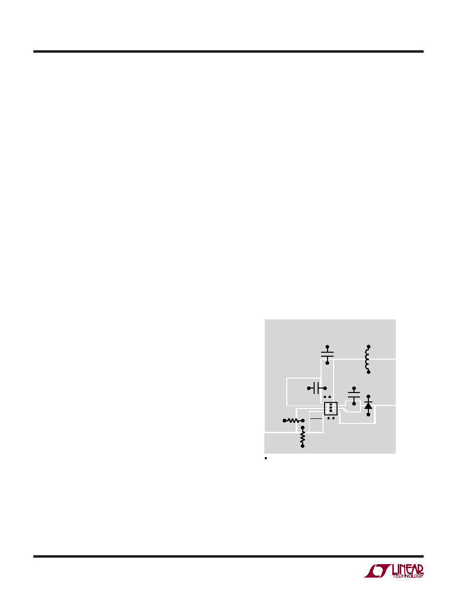
PCB Layout
For proper operation and minimum EMI, care must be taken
during printed circuit board layout. Figure 11 shows the
recommended component placement with trace, ground
plane and via locations. Note that large, switched currents
ow in the LT3502/LT3502A’s VIN and SW pins, the catch
diode (D1) and the input capacitor (C2). The loop formed by
these components should be as small as possible and tied
to system ground in only one place. These components,
along with the inductor and output capacitor, should be
placed on the same side of the circuit board, and their
connections should be made on that layer. Place a local,
unbroken ground plane below these components, and tie
this ground plane to system ground at one location, ideally
at the ground terminal of the output capacitor C1. The SW
and BOOST nodes should be as small as possible. Finally,
keep the FB node small so that the ground pin and ground
traces will shield it from the SW and BOOST nodes. Include
vias near the exposed GND pad of the LT3502/LT3502A
to help remove heat from the LT3502/LT3502A to the
ground plane.
Figure 11
BST
DA
GND
D1
FB
VIN
VOUT
L1
C1
C2
C3
R1
R2
= VIA
3502 F11
BD
SHDN
相关PDF资料 |
PDF描述 |
|---|---|
| LT3502IDC | 1.1 A SWITCHING REGULATOR, 1400 kHz SWITCHING FREQ-MAX, PDSO10 |
| LT3502EDC | 1.1 A SWITCHING REGULATOR, 1400 kHz SWITCHING FREQ-MAX, PDSO10 |
| LT3506IDHD#TR | 3.6 A SWITCHING REGULATOR, 650 kHz SWITCHING FREQ-MAX, PDSO16 |
| LT3506IDHD | 3.6 A SWITCHING REGULATOR, 650 kHz SWITCHING FREQ-MAX, PDSO16 |
| LT3507AIUHF#TRPBF | SWITCHING REGULATOR, PQCC38 |
相关代理商/技术参数 |
参数描述 |
|---|---|
| LT3502AIDC#PBF | 制造商:Linear Technology 功能描述:Conv DC-DC Single Step Down 3V to 40V 8-Pin DFN EP 制造商:Linear Technology 功能描述:Bulk 制造商:Linear Technology 功能描述:DC-DC CONVERTER BUCK 2.2MHZ 制造商:Linear Technology 功能描述:DC-DC CONVERTER, BUCK, 2.2MHZ, DFN-8; Primary Input Voltage:40V; No. of Outputs:1; Output Current:500mA; No. of Pins:8; Operating Temperature Min:-40C; Operating Temperature Max:125C; Operating Temperature Range:-40C to +125C ;RoHS Compliant: Yes |
| LT3502AIDC#TRMPBF | 功能描述:IC REG BUCK ADJ 0.5A 8DFN RoHS:是 类别:集成电路 (IC) >> PMIC - 稳压器 - DC DC 开关稳压器 系列:- 标准包装:250 系列:- 类型:降压(降压) 输出类型:固定 输出数:1 输出电压:1.2V 输入电压:2.05 V ~ 6 V PWM 型:电压模式 频率 - 开关:2MHz 电流 - 输出:500mA 同步整流器:是 工作温度:-40°C ~ 85°C 安装类型:表面贴装 封装/外壳:6-UFDFN 包装:带卷 (TR) 供应商设备封装:6-SON(1.45x1) 产品目录页面:1032 (CN2011-ZH PDF) 其它名称:296-25628-2 |
| LT3502AIDC#TRPBF | 功能描述:IC REG BUCK ADJ 0.5A 8DFN RoHS:是 类别:集成电路 (IC) >> PMIC - 稳压器 - DC DC 开关稳压器 系列:- 标准包装:2,500 系列:- 类型:升压(升压) 输出类型:可调式 输出数:1 输出电压:1.24 V ~ 30 V 输入电压:1.5 V ~ 12 V PWM 型:电流模式,混合 频率 - 开关:600kHz 电流 - 输出:500mA 同步整流器:无 工作温度:-40°C ~ 85°C 安装类型:表面贴装 封装/外壳:8-SOIC(0.154",3.90mm 宽) 包装:带卷 (TR) 供应商设备封装:8-SOIC |
| LT3502AIDC-PBF | 制造商:LINER 制造商全称:Linear Technology 功能描述:1.1MHz/2.2MHz, 500mA Step-Down Regulators in 2mm × 2mm DFN and MS10 |
| LT3502AIDCTRMPBF | 制造商:Linear Technology 功能描述:DC-DC Converter Step-Down 3-40V DFN8EP |
发布紧急采购,3分钟左右您将得到回复。