- 您现在的位置:买卖IC网 > PDF目录14062 > LT3502IMS#PBF (Linear Technology)IC REG BUCK ADJ 0.5A 10MSOP PDF资料下载
参数资料
| 型号: | LT3502IMS#PBF |
| 厂商: | Linear Technology |
| 文件页数: | 13/24页 |
| 文件大小: | 0K |
| 描述: | IC REG BUCK ADJ 0.5A 10MSOP |
| 标准包装: | 50 |
| 类型: | 降压(降压) |
| 输出类型: | 可调式 |
| 输出数: | 1 |
| 输出电压: | 0.8 V ~ 36 V |
| 输入电压: | 3 V ~ 40 V |
| PWM 型: | 电流模式 |
| 频率 - 开关: | 1.1MHz |
| 电流 - 输出: | 500mA |
| 同步整流器: | 无 |
| 工作温度: | -40°C ~ 125°C |
| 安装类型: | 表面贴装 |
| 封装/外壳: | 10-TFSOP,10-MSOP(0.118",3.00mm 宽) |
| 包装: | 管件 |
| 供应商设备封装: | 10-MSOP |
�� �
�
�LT3502/LT3502A�
�APPLICATIONS� INFORMATION�
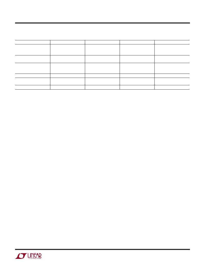
�Table� 2�
�VENDOR�
�Panasonic�
�Kemet�
�Sanyo�
�Murata�
�AVX�
�Taiyo� Yuden�
�PHONE�
�(714)� 373-7366�
�(864)� 963-6300�
�(408)794-9714�
�(404)� 436-1300�
�(864)� 963-6300�
�URL�
�www.panasonic.com�
�www.kemet.com�
�www.sanyovideo.com�
�www.murata.com�
�www.avxcorp.com�
�www.taiyo-yuden.com�
�PART� SERIES�
�Ceramic�
�Polymer,�
�Tantalum�
�Ceramic,�
�Tantalum�
�Ceramic�
�Polymer,�
�Tantalum�
�Ceramic�
�Ceramic,�
�Tantalum�
�Ceramic�
�COMMENTS�
�EEF� Series�
�T494,T495�
�POSCAP�
�TPS� Series�
�13�
�Figure� 4� shows� the� transient� response� of� the� LT3502A� with�
�several� output� capacitor� choices.� The� output� is� 3.3V.� The�
�load� current� is� stepped� from� 150mA� to� 400mA� and� back� to�
�150mA,� and� the� oscilloscope� traces� show� the� output� voltage.�
�The� upper� photo� shows� the� recommended� value.� The� sec-�
�ond� photo� shows� the� improved� response� (less� voltage� drop)�
�resulting� from� a� larger� output� capacitor� and� a� phase� lead�
�capacitor.� The� last� photo� shows� the� response� to� a� high�
�performance� electrolytic� capacitor.� Transient� performance�
�is� improved� due� to� the� large� output� capacitance.�
�BOOST� Pin� Considerations�
�Capacitor� C3� and� the� internal� boost� diode� are� used� to�
�generate� a� boost� voltage� that� is� higher� than� the� input�
�voltage.� In� most� cases� a� 0.1μF� capacitor� will� work� well.�
�Figure� 5� shows� two� ways� to� arrange� the� boost� circuit.� The�
�BOOST� pin� must� be� at� least� 2.2V� above� the� SW� pin� for�
�best� efficiency.� For� outputs� of� 3V� and� above,� the� standard�
�circuit� (Figure� 5a)� is� best.� For� outputs� less� than� 3V� and�
�above� 2.5V,� place� a� discrete� Schottky� diode� (such� as� the�
�BAT54)� in� parallel� with� the� internal� diode� to� reduce� V� D� .� The�
�following� equations� can� be� used� to� calculate� and� minimize�
�boost� capacitance� in� μF:�
�0.012/(V� BD� +� V� CATCH� –� V� D� –� 2.2)� for� the� LT3502A�
�0.030/(V� BD� +� V� CATCH� –� V� D� –� 2.2)� for� the� LT3502�
�V� D� is� the� forward� drop� of� the� boost� diode,� and� V� CATCH� is�
�the� forward� drop� of� the� catch� diode� (D1).�
�For� lower� output� voltages� the� BD� pin� can� be� tied� to� an�
�external� voltage� source� with� adequate� local� bypassing�
�(Figure� 5b).� The� above� equations� still� apply� for� calculating�
�the� optimal� boost� capacitor� for� the� chosen� BD� voltage.�
�The� absence� of� BD� voltage� during� start-up� will� increase�
�minimum� voltage� to� start� and� reduce� efficiency.� You� must�
�also� be� sure� that� the� maximum� voltage� rating� of� BOOST�
�pin� is� not� exceeded.�
�The� minimum� operating� voltage� of� an� LT3502/LT3502A�
�application� is� limited� by� the� undervoltage� lockout� (3V)� and�
�by� the� maximum� duty� cycle� as� outlined� above.� For� proper�
�start-up,� the� minimum� input� voltage� is� also� limited� by� the�
�boost� circuit.� If� the� input� voltage� is� ramped� slowly,� or� the�
�LT3502/LT3502A� is� turned� on� with� its� SHDN� pin� when� the�
�output� is� already� in� regulation,� then� the� boost� capacitor�
�may� not� be� fully� charged.� Because� the� boost� capacitor� is�
�charged� with� the� energy� stored� in� the� inductor,� the� circuit�
�will� rely� on� some� minimum� load� current� to� get� the� boost�
�circuit� running� properly.� This� minimum� load� will� depend�
�on� the� input� and� output� voltages,� and� on� the� arrangement�
�of� the� boost� circuit.� The� minimum� load� generally� goes� to�
�zero� once� the� circuit� has� started.� Figure� 6� shows� plots� of�
�minimum� load� to� start� and� to� run� as� a� function� of� input�
�voltage.� In� many� cases� the� discharged� output� capacitor�
�will� present� a� load� to� the� switcher� which� will� allow� it� to�
�start.� The� plots� show� the� worst-case� situation� where� V� IN�
�is� ramping� very� slowly.� At� light� loads,� the� inductor� current�
�becomes� discontinuous� and� the� effective� duty� cycle� can�
�be� very� high.� This� reduces� the� minimum� input� voltage� to�
�approximately� 400mV� above� V� OUT� .� At� higher� load� currents,�
�the� inductor� current� is� continuous� and� the� duty� cycle� is�
�limited� by� the� maximum� duty� cycle� of� the� LT3502/LT3502A,�
�requiring� a� higher� input� voltage� to� maintain� regulation.�
�3502fd�
�相关PDF资料 |
PDF描述 |
|---|---|
| V24B3V3C100B3 | CONVERTER MOD DC/DC 3.3V 100W |
| LT3502AIMS#PBF | IC REG BUCK ADJ 0.5A 10MSOP |
| V24B3V3C100B2 | CONVERTER MOD DC/DC 3.3V 100W |
| LT3470IDDB#TRPBF | IC REG BUCK ADJ 0.2A 8DFN |
| V24B3V3C100B | CONVERTER MOD DC/DC 3.3V 100W |
相关代理商/技术参数 |
参数描述 |
|---|---|
| LT3502IMS-TRPBF | 制造商:LINER 制造商全称:Linear Technology 功能描述:1.1MHz/2.2MHz, 500mA Step-Down Regulators in 2mm × 2mm DFN and MS10 |
| LT3503 | 制造商:LINER 制造商全称:Linear Technology 功能描述:1A, 2.2MHz Step-Down Switching Regulator in 2mm × 3mm DFN |
| LT3503EDCB | 制造商:LINER 制造商全称:Linear Technology 功能描述:1A, 2.2MHz Step-Down Switching Regulator in 2mm × 3mm DFN |
| LT3503EDCB#PBF | 制造商:Linear Technology 功能描述:Conv DC-DC Single Step Down 3.6V to 20V 6-Pin DFN EP 制造商:Linear Technology 功能描述:REG SWITCHING STEP DOWN 1A 2.2MHZ 制造商:Linear Technology 功能描述:REG, SWITCHING, STEP DOWN, 1A 2.2MHZ 制造商:Linear Technology 功能描述:SP-SWREG/Monolithic, Cut Tape 1A, 2.2MHz Buck Regulator ;RoHS Compliant: Yes |
| LT3503EDCB#TR | 制造商:Linear Technology 功能描述:Conv DC-DC Single Step Down 3.6V to 20V 6-Pin DFN EP T/R |
发布紧急采购,3分钟左右您将得到回复。