- 您现在的位置:买卖IC网 > PDF目录14855 > LT3503EDCB#TRMPBF (Linear Technology)IC REG BUCK ADJ 1A 6DFN PDF资料下载
参数资料
| 型号: | LT3503EDCB#TRMPBF |
| 厂商: | Linear Technology |
| 文件页数: | 8/20页 |
| 文件大小: | 0K |
| 描述: | IC REG BUCK ADJ 1A 6DFN |
| 标准包装: | 1 |
| 类型: | 降压(降压) |
| 输出类型: | 可调式 |
| 输出数: | 1 |
| 输出电压: | 0.78 V ~ 16.2 V |
| 输入电压: | 3.6 V ~ 20 V |
| PWM 型: | 电流模式 |
| 频率 - 开关: | 2.2MHz |
| 电流 - 输出: | 1A |
| 同步整流器: | 无 |
| 工作温度: | -40°C ~ 85°C |
| 安装类型: | 表面贴装 |
| 封装/外壳: | 6-WFDFN 裸露焊盘 |
| 包装: | 标准包装 |
| 供应商设备封装: | 6-DFN-EP(2x3) |
| 产品目录页面: | 1331 (CN2011-ZH PDF) |
| 其它名称: | LT3503EDCB#TRMPBFDKR |
�� �
�
�LT3503�
�APPLICATIO� S� I� FOR� ATIO�
�R� 1� =� R� 2� ?� OUT� –� 1� ?�
�FB Resistor Network�
�The� output� voltage� is� programmed� with� a� resistor� divider�
�between� the� output� and� the� FB� pin.� Choose� the� 1%�
�resistors� according� to:�
�?� V� ?�
�?� 0� .� 78� V� ?�
�R2� should� be� 20.0k� or� less� to� avoid� bias� current� errors.�
�Reference� designators� refer� to� the� Block� Diagram.�
�An� optional� phase� lead� capacitor� of� 22pF� between� V� OUT�
�and� FB� reduces� light-load� output� ripple.�
�Input� Voltage� Range�
�The� input� voltage� range� for� LT3503� applications� depends�
�on� the� output� voltage� and� on� the� absolute� maximum�
�ratings� of� the� V� IN� and� BOOST� pins.�
�The� minimum� input� voltage� is� determined� by� either� the�
�LT3503’s� minimum� operating� voltage� of� 3.6V,� or� by� its�
�maximum� duty� cycle.� The� duty� cycle� is� the� fraction� of� time�
�that� the� internal� switch� is� on� and� is� determined� by� the� input�
�and� output� voltages:�
�In� pulse-skipping� mode� the� part� skips� pulses� to� control� the�
�inductor� current� and� regulate� the� output� voltage,� possibly�
�producing� a� spectrum� of� frequencies� below� 2.2MHz.�
�Note� that� this� is� a� restriction� on� the� operating� input� voltage�
�to� remain� in� constant-frequency� operation;� the� circuit� will�
�tolerate� transient� inputs� up� to� the� absolute� maximum�
�ratings� of� the� V� IN� and� BOOST� pins� when� the� output� is� in�
�regulation.� The� input� voltage� should� be� limited� to� V� IN(PS)�
�during� overload� conditions� (short-circuit� or� start-up).�
�Minimum� On� Time�
�The� part� will� still� regulate� the� output� at� input� voltages� that�
�exceed� V� IN(PS)� (up� to� 20V),� but� the� output� voltage� ripple�
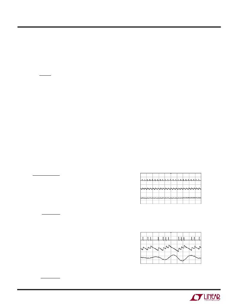
�increases.� Figure� 1� illustrates� switching� waveforms� in�
�continuous� mode� for� a� 0.78V� output� application� near�
�V� IN(PS)� =� 6V.�
�As� the� input� voltage� is� increased,� the� part� is� required� to�
�switch� for� shorter� periods� of� time.� Delays� associated� with�
�turning� off� the� power� switch� dictate� the� minimum� on� time�
�of� the� part.� The� minimum� on� time� for� the� LT3503� is�
�~130ns.� Figure� 2� illustrates� the� switching� waveforms�
�when� the� input� voltage� is� increased� to� V� IN� =� 14V.�
�DC� =�
�V� OUT� +� V� D�
�V� IN� –� V� SW� +� V� D�
�V� SW�
�10V/DIV�
�where� V� D� is� the� forward� voltage� drop� of� the� catch� diode�
�(~0.4V)� and� V� SW� is� the� voltage� drop� of� the� internal� switch�
�(~0.4V� at� maximum� load).� This� leads� to� a� minimum� input�
�I� L�
�1A/DIV�
�V� OUT�
�20mV/DIV�
�voltage� of:�
�V� IN� (� MIN� )� =�
�V� OUT� +� V� D�
�DC� MAX�
�–� V� D� +� V� SW�
�C� OUT� =� 47� μ� F�
�V� OUT� =� 0.78V�
�V� IN� =� 7V�
�I� LOAD� =� 1.1A�
�L� =� 1.1� μ� H�
�1� μ� s/DIV�
�3503� F01�
�with� DC� MAX� =� 0.81� (0.76� over� temperature).�
�The� maximum� input� voltage� is� determined� by� the� absolute�
�maximum� ratings� of� the� V� IN� and� BOOST� pins.� For� con-�
�stant-frequency� operation� the� maximum� input� voltage� is�
�determined� by� the� minimum� duty� cycle,� DC� MIN� =� 0.29.� If�
�V� SW�
�10V/DIV�
�I� L�
�1A/DIV�
�Figure� 1�
�the� duty� cycle� requirement� is� less� than� DC� MIN� ,� the� part� will�
�enter� pulse-skipping� mode.� The� onset� of� pulse-skipping�
�occurs� at:�
�V� OUT�
�20mV/DIV�
�C� OUT� =� 47� μ� F�
�V� OUT� =� 0.78V�
�1� μ� s/DIV�
�3503� F02�
�V� IN� (� PS� )� =�
�V� OUT� +� V� D�
�DC� MIN�
�–� V� D� +� V� SW�
�V� IN� =� 14V�
�I� LOAD� =� 1.1A�
�L� =� 1.1� μ� H�
�Figure� 2�
�3503f�
�8�
�相关PDF资料 |
PDF描述 |
|---|---|
| SLP392M080H3P3 | CAP ALUM 3900UF 80V 20% SNAP |
| LPX561M160C3P3 | CAP ALUM 560UF 160V 20% SNAP |
| GCM36DCCN-S189 | CONN EDGECARD 72POS R/A .156 SLD |
| ESRD121M06XB | CAP ALUM 120UF 6.3V 20% SMD |
| LLS2A222MELZ | CAP ALUM 2200UF 100V 20% SNAP |
相关代理商/技术参数 |
参数描述 |
|---|---|
| LT3504 | 制造商:LINER 制造商全称:Linear Technology 功能描述:Quad 40V/1A Step-Down Switching Regulator |
| LT3504EUFD#PBF | 功能描述:IC REG BUCK ADJ 1A QUAD 28-QFN RoHS:是 类别:集成电路 (IC) >> PMIC - 稳压器 - DC DC 开关稳压器 系列:- 设计资源:Design Support Tool 标准包装:1 系列:- 类型:升压(升压) 输出类型:固定 输出数:1 输出电压:3V 输入电压:0.75 V ~ 2 V PWM 型:- 频率 - 开关:- 电流 - 输出:100mA 同步整流器:是 工作温度:-40°C ~ 85°C 安装类型:表面贴装 封装/外壳:SOT-23-5 细型,TSOT-23-5 包装:剪切带 (CT) 供应商设备封装:TSOT-23-5 其它名称:AS1323-BTTT-30CT |
| LT3504EUFD#TRPBF | 功能描述:IC REG BUCK ADJ 1A QUAD 28-QFN RoHS:是 类别:集成电路 (IC) >> PMIC - 稳压器 - DC DC 开关稳压器 系列:- 设计资源:Design Support Tool 标准包装:1 系列:- 类型:升压(升压) 输出类型:固定 输出数:1 输出电压:3V 输入电压:0.75 V ~ 2 V PWM 型:- 频率 - 开关:- 电流 - 输出:100mA 同步整流器:是 工作温度:-40°C ~ 85°C 安装类型:表面贴装 封装/外壳:SOT-23-5 细型,TSOT-23-5 包装:剪切带 (CT) 供应商设备封装:TSOT-23-5 其它名称:AS1323-BTTT-30CT |
| LT3504IUFD#PBF | 功能描述:IC REG BUCK ADJ 1A QUAD 28-QFN RoHS:是 类别:集成电路 (IC) >> PMIC - 稳压器 - DC DC 开关稳压器 系列:- 设计资源:Design Support Tool 标准包装:1 系列:- 类型:升压(升压) 输出类型:固定 输出数:1 输出电压:3V 输入电压:0.75 V ~ 2 V PWM 型:- 频率 - 开关:- 电流 - 输出:100mA 同步整流器:是 工作温度:-40°C ~ 85°C 安装类型:表面贴装 封装/外壳:SOT-23-5 细型,TSOT-23-5 包装:剪切带 (CT) 供应商设备封装:TSOT-23-5 其它名称:AS1323-BTTT-30CT |
| LT3504IUFD#TRPBF | 功能描述:IC REG BUCK ADJ 1A QUAD 28-QFN RoHS:是 类别:集成电路 (IC) >> PMIC - 稳压器 - DC DC 开关稳压器 系列:- 设计资源:Design Support Tool 标准包装:1 系列:- 类型:升压(升压) 输出类型:固定 输出数:1 输出电压:3V 输入电压:0.75 V ~ 2 V PWM 型:- 频率 - 开关:- 电流 - 输出:100mA 同步整流器:是 工作温度:-40°C ~ 85°C 安装类型:表面贴装 封装/外壳:SOT-23-5 细型,TSOT-23-5 包装:剪切带 (CT) 供应商设备封装:TSOT-23-5 其它名称:AS1323-BTTT-30CT |
发布紧急采购,3分钟左右您将得到回复。