- 您现在的位置:买卖IC网 > PDF目录20624 > LT3507EUHF#TRPBF (Linear Technology)IC REG QD BUCK/LINEAR 38-QFN PDF资料下载
参数资料
| 型号: | LT3507EUHF#TRPBF |
| 厂商: | Linear Technology |
| 文件页数: | 19/28页 |
| 文件大小: | 302K |
| 描述: | IC REG QD BUCK/LINEAR 38-QFN |
| 产品培训模块: | More Information on LDOs |
| 标准包装: | 2,500 |
| 拓扑: | 降压(降压)(1),线性(LDO)(1) |
| 功能: | 任何功能 |
| 输出数: | 4 |
| 频率 - 开关: | 900kHz ~ 1.1MHz |
| 电压/电流 - 输出 1: | 0.8 V ~ 32.4 V,2.4A |
| 电压/电流 - 输出 2: | 0.8 V ~ 32.4 V,1.5A |
| 电压/电流 - 输出 3: | 0.8 V ~ 32.4 V,1.5A |
| 带 LED 驱动器: | 无 |
| 带监控器: | 无 |
| 带序列发生器: | 是 |
| 电源电压: | 4 V ~ 36 V |
| 工作温度: | -40°C ~ 125°C |
| 安装类型: | 表面贴装 |
| 封装/外壳: | 38-WFQFN 裸露焊盘 |
| 供应商设备封装: | 38-QFN(5x7) |
| 包装: | 带卷 (TR) |
第1页第2页第3页第4页第5页第6页第7页第8页第9页第10页第11页第12页第13页第14页第15页第16页第17页第18页当前第19页第20页第21页第22页第23页第24页第25页第26页第27页第28页
LT3507
19
3507fa
the TRK/SS2 voltage is substantially higher than 0.8V at
steady state and effectively turns off D1. D2 and D3 will
therefore conduct the same current and offer tight matching
between V
FB2
and the internal precision 0.8V reference. In
the ratiometric mode with R6 = R2, TRK/SS2 equals 0.8V
at steady state. D1 will divert part of the bias current and
make V
FB2
slightly lower than 0.8V. Although this error
is minimized by the exponential I-V characteristic of the
diodes, it does impose a nite amount of output voltage
deviation. Further, when channel 1s output experiences
dynamic excursions (under load transient, for example),
channel 2 will be affected as well. Setting R6 to a value
that pushes the TRK/SS2 voltage to 1V at steady state will
eliminate these problems while providing near ratiometric
tracking.
The example shows channel 2 tracking channel 1, however
any channel may be set up to track any other channel.
If a capacitor is tied from the TRK/SS pin to ground, then
the internal pull-up current will generate a voltage ramp on
this pin. This results in a ramp at the output, limiting the
inductor current and therefore input current during start-up.
A good value for the soft-start capacitor is C
OUT
/10,000,
where C
OUT
is the value of the output capacitor.
MULTIPLE INPUT SUPPLIES
V
IN1
, V
IN2
and V
IN3
are independent and can be powered
with different voltages provided V
IN1
is present when V
IN2
or V
IN3
is present. Each supply must be bypassed as close
to the V
IN
pins as possible.
For applications requiring large inductors due to high V
IN
to V
OUT
ratios, a 2-stage step-down approach may reduce
inductor size by allowing an increase in frequency. A dual
step-down application steps down the input voltage (V
IN1
)
to the highest output voltage, then uses that voltage to
power the other outputs (V
IN2
and V
IN3
). V
OUT1
must be
able to provide enough current for its output plus the
input current at V
IN2
and V
IN3
when V
OUT2
and V
OUT3
are
at maximum load. The Typical Applications section shows
a 36V to 15V, 1.8V and 1.2V 2-stage converter using this
approach.
For applications with multiple voltages, the LT3507 can
accommodate input voltages as low as 3V on V
IN2
and
APPLICATIONS INFORMATION
V
IN3
. This can be useful in applications regulating outputs
from a PCI Express bus, where the 12V input is power
limited and the 3.3V input has power available to drive
other outputs. In this case, tie the 12V input to V
IN1
and
the 3.3V input to V
IN2
and V
IN3
.
LOW DROPOUT REGULATOR
The low dropout regulator comprises an error amp, loop
compensation and a base drive amp. It uses the same
0.8V reference as the switching regulators. It requires an
external NPN pass transistor and 2.2糉 of output capaci-
tance for stability.
The dropout characteristics will be determined by the pass
transistor. The collector-emitter saturation characteristics
will limit the dropout voltage. Table 4 lists some suitable
NPN transistors with their saturation speci cations.
The base drive voltage has a maximum voltage of 5V.
This will limit the maximum output of the regulator to
5V V
BESAT
where V
BESAT
is the base-emitter saturation
voltage of the pass transistor.
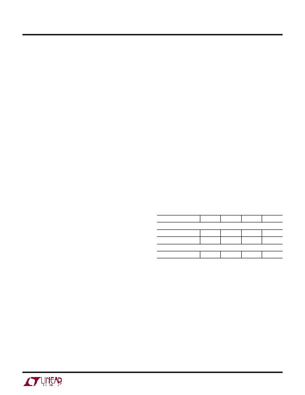
Table 4. NPN Pass Transistors and Saturation Characteristics
PART NUMBER
V
CESAT
V
BESAT
I
C
(mA) I
B
(mA)
On Semiconductor
NSS30071
0.25 0.85 500
5
NSS30101
0.2 0.85 1000 10
Fairchild
KSC3265
0.4
500 20
The LDO is always on when any of the switcher channels
is on. The LDO may be shut down if it is unused by pull-
ing the FB4 pin up with a 30糀 current source. The FB4
pin will clamp at about 1.25V and the LDO will shut off
reducing power consumption. This pull-up can be sourced
from one of the LT3507 outputs provided that channel is
always on when the other channels are on.
The output stage of the LDO will drive the NPN base from
the BIAS voltage if it is at least 0.8V above the LDO DRIVE
voltage.
FB Resistor Network
The output voltage of the LDO regulator is programmed
with a resistor divider (Refer to Block Diagram) between the
相关PDF资料 |
PDF描述 |
|---|---|
| ADE7953ACPZ-RL | IC ENERGY METERING 1PH 28LFCSP |
| LT3694IUFD-1#TRPBF | IC REG TRPL BUCK/LINEAR 28QFN |
| 591D687X0004R2T20H | CAP TANT 680UF 4V 20% 2824 |
| LT3694IUFD#TRPBF | IC REG TRPL BUCK/LINEAR 28QFN |
| GMA50DTMZ-S664 | CONN EDGECARD 100PS R/A .125 SLD |
相关代理商/技术参数 |
参数描述 |
|---|---|
| LT3507HUHF#PBF | 功能描述:IC REG QD BUCK/LINEAR 38-QFN RoHS:是 类别:集成电路 (IC) >> PMIC - 稳压器 - 线性 + 切换式 系列:- 标准包装:2,500 系列:- 拓扑:降压(降压)同步(3),线性(LDO)(2) 功能:任何功能 输出数:5 频率 - 开关:300kHz 电压/电流 - 输出 1:控制器 电压/电流 - 输出 2:控制器 电压/电流 - 输出 3:控制器 带 LED 驱动器:无 带监控器:无 带序列发生器:是 电源电压:5.6 V ~ 24 V 工作温度:-40°C ~ 85°C 安装类型:* 封装/外壳:* 供应商设备封装:* 包装:* |
| LT3507HUHF#TRPBF | 功能描述:IC REG QD BUCK/LINEAR 38-QFN RoHS:是 类别:集成电路 (IC) >> PMIC - 稳压器 - 线性 + 切换式 系列:- 标准包装:2,500 系列:- 拓扑:降压(降压)同步(3),线性(LDO)(2) 功能:任何功能 输出数:5 频率 - 开关:300kHz 电压/电流 - 输出 1:控制器 电压/电流 - 输出 2:控制器 电压/电流 - 输出 3:控制器 带 LED 驱动器:无 带监控器:无 带序列发生器:是 电源电压:5.6 V ~ 24 V 工作温度:-40°C ~ 85°C 安装类型:* 封装/外壳:* 供应商设备封装:* 包装:* |
| LT3507HUHF-PBF | 制造商:LINER 制造商全称:Linear Technology 功能描述:Triple Monolithic Step-Down Regulator with LDO |
| LT3507HUHF-TRPBF | 制造商:LINER 制造商全称:Linear Technology 功能描述:Triple Monolithic Step-Down Regulator with LDO |
| LT3507IUHF#PBF | 功能描述:IC REG QD BUCK/LINEAR 38-QFN RoHS:是 类别:集成电路 (IC) >> PMIC - 稳压器 - 线性 + 切换式 系列:- 标准包装:2,500 系列:- 拓扑:降压(降压)同步(3),线性(LDO)(2) 功能:任何功能 输出数:5 频率 - 开关:300kHz 电压/电流 - 输出 1:控制器 电压/电流 - 输出 2:控制器 电压/电流 - 输出 3:控制器 带 LED 驱动器:无 带监控器:无 带序列发生器:是 电源电压:5.6 V ~ 24 V 工作温度:-40°C ~ 85°C 安装类型:* 封装/外壳:* 供应商设备封装:* 包装:* |
发布紧急采购,3分钟左右您将得到回复。