- 您现在的位置:买卖IC网 > PDF目录44984 > LT3508IFE#TR (LINEAR TECHNOLOGY CORP) 3.2 A DUAL SWITCHING CONTROLLER, 1060 kHz SWITCHING FREQ-MAX, PDSO16 PDF资料下载
参数资料
| 型号: | LT3508IFE#TR |
| 厂商: | LINEAR TECHNOLOGY CORP |
| 元件分类: | 稳压器 |
| 英文描述: | 3.2 A DUAL SWITCHING CONTROLLER, 1060 kHz SWITCHING FREQ-MAX, PDSO16 |
| 封装: | 4.40 MM, PLASTIC, TSSOP-16 |
| 文件页数: | 5/24页 |
| 文件大小: | 365K |
| 代理商: | LT3508IFE#TR |
LT3508
13
3508f
Peak reverse voltage is equal to the regulator input voltage.
Use a diode with a reverse voltage rating greater than the
input voltage. Table 4 lists several Schottky diodes and their
manufacturers. If operating at high ambient temperatures,
consider using a Schottky with low reverse leakage.
Table 4. Schottky Diodes
PART NUMBER
VR
(V)
IAVE
(A)
VF at 1A
(mV)
VF at 2A
(mV)
On Semiconductor
MBR0520L
20
0.5
MBR0540
40
0.5
620
MBRM120E
20
1
530
MBRM140
40
1
550
Diodes Inc.
B0530W
30
0.5
B120
20
1
500
B130
30
1
500
B140HB
40
1
DFLS140
40
1.1
510
B240
40
2
500
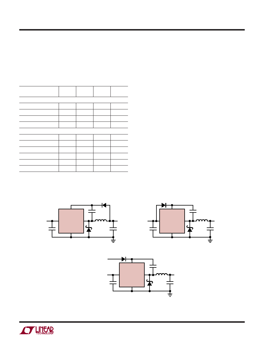
BOOST Pin Considerations
The capacitor and diode tied to the BOOST pin generate
a voltage that is higher than the input voltage. In most
cases, a 0.22F capacitor and fast switching diode (such
as the CMDSH-3 or MMSD914LT1) will work well. For ap-
plications 1MHz or faster, a 0.1F capacitor is sufcient.
Use a 0.47F capacitor or greater for applicaitons running
below 500kHz. Figure 4 shows three ways to arrange the
boost circuit. The BOOST pin must be more than 2.5V
above the SW pin for full efciency. For outputs of 3.3V
and higher, the standard circuit (Figure 4a) is best. For
outputs between 2.8V and 3.3V, use a small Schottky diode
(such as the BAT-54). For lower output voltages, the boost
diode can be tied to the input (Figure 4b). The circuit in
Figure 4a is more efcient because the boost pin current
comes from a lower voltage source. Finally, the anode of
the boost diode can be tied to another source that is at
least 3V (Figure 4c). For example, if you are generating
a 3.3V output, and the 3.3V output is on whenever the
particular channel is on, the anode of the BOOST diode
can be connected to the 3.3V output. In any case, be sure
that the maximum voltage at the BOOST pin is both less
than 60V and the voltage difference between the BOOST
and SW pins is less than 30V.
APPLICATIONS INFORMATION
VIN
BOOST
GND
SW
VIN
LT3508
(4a)
D2
VOUT
C3
VBOOST – VSW VOUT
MAX VBOOST VIN + VOUT
VIN
BOOST
GND
SW
VIN
LT3508
(4b)
D2
VOUT
C3
VBOOST – VSW VIN
MAX VBOOST 2VIN
D2
VIN
BOOST
GND
SW
VIN
LT3508
(4c)
3508 F04
VOUT
VBOOST – VSW VIN2
MAX VBOOST VIN2 + VIN
MINIMUM VALUE FOR VIN2 = 3V
VIN2 > 3V
C3
Figure 4. Generating the Boost Voltage
相关PDF资料 |
PDF描述 |
|---|---|
| LT3508EUF | 3.2 A DUAL SWITCHING CONTROLLER, 1060 kHz SWITCHING FREQ-MAX, PQCC24 |
| LT3509HMSE#TRPBF | 1.2 A DUAL SWITCHING CONTROLLER, 2500 kHz SWITCHING FREQ-MAX, PDSO16 |
| LT3509IMSE#PBF | 1.2 A DUAL SWITCHING CONTROLLER, 2500 kHz SWITCHING FREQ-MAX, PDSO16 |
| LT3509IMSE#TRPBF | 1.2 A DUAL SWITCHING CONTROLLER, 2500 kHz SWITCHING FREQ-MAX, PDSO16 |
| LT3509EMSE#TRPBF | 1.2 A DUAL SWITCHING CONTROLLER, 2500 kHz SWITCHING FREQ-MAX, PDSO16 |
相关代理商/技术参数 |
参数描述 |
|---|---|
| LT3508IFE-TRPBF | 制造商:LINER 制造商全称:Linear Technology 功能描述:Dual Monolithic 1.4A Step-Down Switching Regulator |
| LT3508IUF#PBF | 功能描述:IC REG BUCK ADJ 1.4A DL 24QFN RoHS:是 类别:集成电路 (IC) >> PMIC - 稳压器 - DC DC 开关稳压器 系列:- 标准包装:250 系列:- 类型:降压(降压) 输出类型:固定 输出数:1 输出电压:1.2V 输入电压:2.05 V ~ 6 V PWM 型:电压模式 频率 - 开关:2MHz 电流 - 输出:500mA 同步整流器:是 工作温度:-40°C ~ 85°C 安装类型:表面贴装 封装/外壳:6-UFDFN 包装:带卷 (TR) 供应商设备封装:6-SON(1.45x1) 产品目录页面:1032 (CN2011-ZH PDF) 其它名称:296-25628-2 |
| LT3508IUF#PBF | 制造商:Linear Technology 功能描述:DC-DC CONVERTER BUCK 1MHZ Q 制造商:Linear Technology 功能描述:DC-DC CONVERTER, BUCK, 1MHZ, QFN-24 |
| LT3508IUF#TRPBF | 功能描述:IC REG BUCK ADJ 1.4A DL 24QFN RoHS:是 类别:集成电路 (IC) >> PMIC - 稳压器 - DC DC 开关稳压器 系列:- 设计资源:Design Support Tool 标准包装:1 系列:- 类型:升压(升压) 输出类型:固定 输出数:1 输出电压:3V 输入电压:0.75 V ~ 2 V PWM 型:- 频率 - 开关:- 电流 - 输出:100mA 同步整流器:是 工作温度:-40°C ~ 85°C 安装类型:表面贴装 封装/外壳:SOT-23-5 细型,TSOT-23-5 包装:剪切带 (CT) 供应商设备封装:TSOT-23-5 其它名称:AS1323-BTTT-30CT |
| LT3508IUF-PBF | 制造商:LINER 制造商全称:Linear Technology 功能描述:Dual Monolithic 1.4A Step-Down Switching Regulator |
发布紧急采购,3分钟左右您将得到回复。