- 您现在的位置:买卖IC网 > PDF目录44984 > LT3508IUF#TR (LINEAR TECHNOLOGY CORP) 3.2 A DUAL SWITCHING CONTROLLER, 1060 kHz SWITCHING FREQ-MAX, PQCC24 PDF资料下载
参数资料
| 型号: | LT3508IUF#TR |
| 厂商: | LINEAR TECHNOLOGY CORP |
| 元件分类: | 稳压器 |
| 英文描述: | 3.2 A DUAL SWITCHING CONTROLLER, 1060 kHz SWITCHING FREQ-MAX, PQCC24 |
| 封装: | 4 X 4 MM, PLASTIC, MO-220WGGD-X, QFN-24 |
| 文件页数: | 10/24页 |
| 文件大小: | 365K |
| 代理商: | LT3508IUF#TR |
LT3508
18
3508f
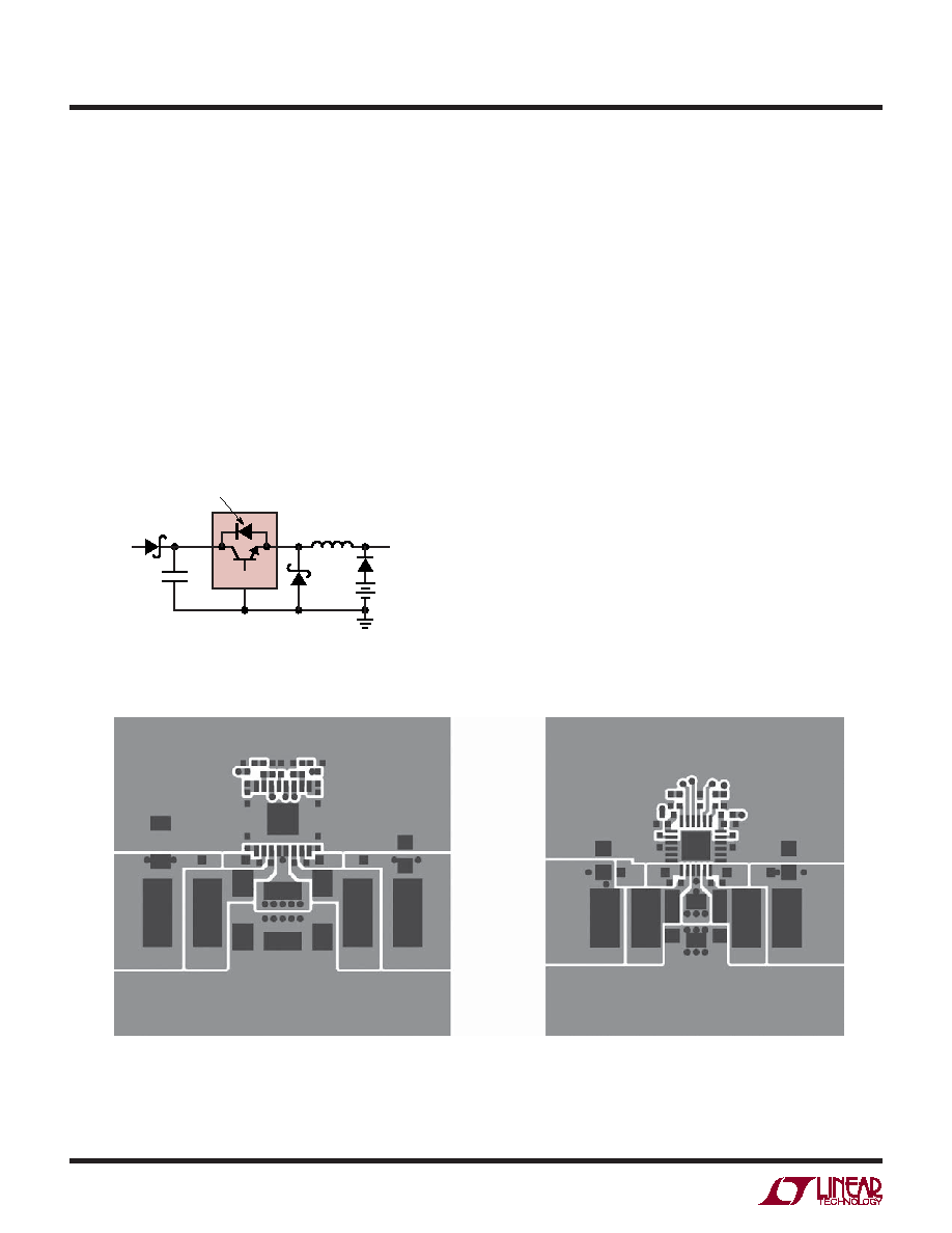
applications or in battery back-up systems where a battery
or some other supply is diode OR-ed with the LT3508’s
output. If the VIN pin is allowed to oat and the SHDN pin
is held high (either by a logic signal or because it is tied
to VIN), then the LT3508’s internal circuitry will pull its
quiescent current through its SW pin. This is ne if your
system can tolerate a few mA in this state. If you ground
the
SHDN pin, the SW pin current will drop to essentially
zero. However, if the VIN pin is grounded while the output
is held high, then parasitic diodes inside the LT3508 can
pull large currents from the output through the SW pin
and the VIN pin. Figure 10 shows a circuit that will run
only when the input voltage is present and that protects
against a shorted or reversed input.
APPLICATIONS INFORMATION
Figure 11. A Good PCB Layout Ensures Proper Low EMI Operation
PCB Layout
For proper operation and minimum EMI, care must be taken
during printed circuit board layout. Figure 11 shows the
recommended PCB layout with trace and via locations. Note
that large, switched currents ow in the LT3508’s VIN and
SW pins, the catch diode (D1) and the input capacitor (CIN).
The loop formed by these components should be as small
as possible. These components, along with the inductor
and output capacitor, should be placed on the same side
of the circuit board, and their connections should be made
on that layer. Place a local, unbroken ground plane below
these components. The SW and BOOST nodes should be as
small as possible. Finally, keep the FB and VC nodes small
so that the ground traces will shield them from the SW
and BOOST nodes. The Exposed Pad on the bottom of the
package must be soldered to ground so that the pad acts
as a heat sink. To keep thermal resistance low, extend the
ground plane as much as possible, and add thermal vias
under and near the LT3508 to additional ground planes
within the circuit board and on the bottom side.
VIN
VOUT
SW
LT3508
D4
PARASITIC DIODE
3508 F10
Figure 10. Diode D4 Prevents a Shorted Input from Discharging
a Backup Battery Tied to the Output
(11a) Example Layout for FE16 Package
(11b) Example Layout for QFN Package
相关PDF资料 |
PDF描述 |
|---|---|
| LT3508IUF | 3.2 A DUAL SWITCHING CONTROLLER, 1060 kHz SWITCHING FREQ-MAX, PQCC24 |
| LT3508IFE#TR | 3.2 A DUAL SWITCHING CONTROLLER, 1060 kHz SWITCHING FREQ-MAX, PDSO16 |
| LT3508EUF | 3.2 A DUAL SWITCHING CONTROLLER, 1060 kHz SWITCHING FREQ-MAX, PQCC24 |
| LT3509HMSE#TRPBF | 1.2 A DUAL SWITCHING CONTROLLER, 2500 kHz SWITCHING FREQ-MAX, PDSO16 |
| LT3509IMSE#PBF | 1.2 A DUAL SWITCHING CONTROLLER, 2500 kHz SWITCHING FREQ-MAX, PDSO16 |
相关代理商/技术参数 |
参数描述 |
|---|---|
| LT3508IUF-TRPBF | 制造商:LINER 制造商全称:Linear Technology 功能描述:Dual Monolithic 1.4A Step-Down Switching Regulator |
| LT3509 | 制造商:LINER 制造商全称:Linear Technology 功能描述:36V 500mA Step-Down Regulator and 200mA LDO |
| LT3509EDE#PBF | 功能描述:IC REG BUCK ADJ 0.7A DL 14DFN RoHS:是 类别:集成电路 (IC) >> PMIC - 稳压器 - DC DC 开关稳压器 系列:- 标准包装:250 系列:- 类型:降压(降压) 输出类型:固定 输出数:1 输出电压:1.2V 输入电压:2.05 V ~ 6 V PWM 型:电压模式 频率 - 开关:2MHz 电流 - 输出:500mA 同步整流器:是 工作温度:-40°C ~ 85°C 安装类型:表面贴装 封装/外壳:6-UFDFN 包装:带卷 (TR) 供应商设备封装:6-SON(1.45x1) 产品目录页面:1032 (CN2011-ZH PDF) 其它名称:296-25628-2 |
| LT3509EDE#TRPBF | 功能描述:IC REG BUCK ADJ 0.7A DL 14DFN RoHS:是 类别:集成电路 (IC) >> PMIC - 稳压器 - DC DC 开关稳压器 系列:- 标准包装:2,500 系列:- 类型:降压(降压) 输出类型:固定 输出数:1 输出电压:1.2V,1.5V,1.8V,2.5V 输入电压:2.7 V ~ 20 V PWM 型:- 频率 - 开关:- 电流 - 输出:50mA 同步整流器:是 工作温度:-40°C ~ 125°C 安装类型:表面贴装 封装/外壳:10-TFSOP,10-MSOP(0.118",3.00mm 宽)裸露焊盘 包装:带卷 (TR) 供应商设备封装:10-MSOP 裸露焊盘 |
| LT3509EDEPBF | 制造商:Linear Technology 功能描述:Sw. Regulator Dual 700mA 3.6-36V DFN14EP |
发布紧急采购,3分钟左右您将得到回复。