- 您现在的位置:买卖IC网 > PDF目录13904 > LT3508IUF#TRPBF (Linear Technology)IC REG BUCK ADJ 1.4A DL 24QFN PDF资料下载
参数资料
| 型号: | LT3508IUF#TRPBF |
| 厂商: | Linear Technology |
| 文件页数: | 14/26页 |
| 文件大小: | 0K |
| 描述: | IC REG BUCK ADJ 1.4A DL 24QFN |
| 标准包装: | 2,500 |
| 类型: | 降压(降压) |
| 输出类型: | 可调式 |
| 输出数: | 2 |
| 输出电压: | 0.8 V ~ 35.3 V |
| 输入电压: | 3.7 V ~ 36 V |
| PWM 型: | 电流模式 |
| 频率 - 开关: | 920kHz ~ 1.06MHz |
| 电流 - 输出: | 1.4A |
| 同步整流器: | 无 |
| 工作温度: | -40°C ~ 125°C |
| 安装类型: | 表面贴装 |
| 封装/外壳: | 24-WFQFN 裸露焊盘 |
| 包装: | 带卷 (TR) |
| 供应商设备封装: | 24-QFN 裸露焊盘(4x4) |
�� �
�
�LT3508�
�APPLICATIONS� INFORMATION�
�The� minimum� operating� voltage� of� an� LT3508� applica-�
�tion� is� limited� by� the� undervoltage� lockout� (≈3.7V)� and�
�by� the� maximum� duty� cycle.� The� boost� circuit� also� limits�
�the� minimum� input� voltage� for� proper� start-up.� If� the�
�input� voltage� ramps� slowly,� or� the� LT3508� turns� on� when�
�the� output� is� already� in� regulation,� the� boost� capacitor�
�may� not� be� fully� charged.� Because� the� boost� capacitor�
�charges� with� the� energy� stored� in� the� inductor,� the� circuit�
�will� rely� on� some� minimum� load� current� to� get� the� boost�
�circuit� running� properly.� This� minimum� load� will� depend�
�on� input� and� output� voltages,� and� on� the� arrangement� of�
�the� boost� circuit.� The� minimum� load� current� generally�
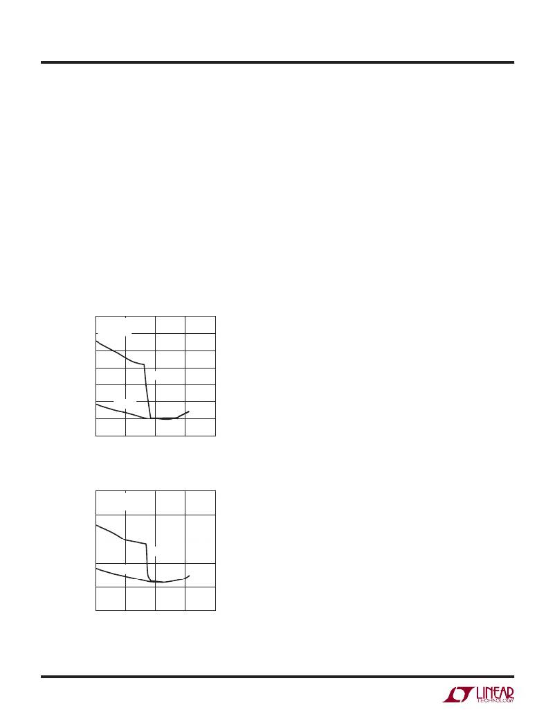
�goes� to� zero� once� the� circuit� has� started.� Figure� 5� shows�
�a� plot� of� minimum� load� to� start� and� to� run� as� a� function�
�of� input� voltage.� Even� without� an� output� load� current,� in�
�Minimum� Input� Voltage,� V� OUT� =� 3.3V�
�many� cases� the� discharged� output� capacitor� will� present�
�a� load� to� the� switcher� that� will� allow� it� to� start.� The� plots�
�show� the� worst� case,� where� V� IN� is� ramping� very� slowly.�
�Frequency� Compensation�
�The� LT3508� uses� current� mode� control� to� regulate� the�
�output.� This� simpli?es� loop� compensation.� In� particular,� the�
�LT3508� does� not� require� the� ESR� of� the� output� capacitor�
�for� stability,� so� you� are� free� to� use� ceramic� capacitors� to�
�achieve� low� output� ripple� and� small� circuit� size.�
�Frequency� compensation� is� provided� by� the� components�
�tied� to� the� V� C� pin,� as� shown� in� Figure� 1.� Generally� a� capaci-�
�tor� (C� C� )� and� a� resistor� (R� C� )� in� series� to� ground� are� used.� In�
�addition,� there� may� be� a� lower� value� capacitor� in� parallel.�
�This� capacitor� (C� F� )� is� not� part� of� the� loop� compensation�
�but� is� used� to� ?lter� noise� at� the� switching� frequency,� and�
�6.5�
�6.0�
�5.5�
�5.0�
�4.5�
�4.0�
�3.5�
�T� A� =� 25°C�
�V� OUT� =� 3.3V�
�TO� RUN�
�TO� START�
�is� required� only� if� a� phase-lead� capacitor� is� used� or� if� the�
�output� capacitor� has� high� ESR.�
�Loop� compensation� determines� the� stability� and� transient�
�performance.� Designing� the� compensation� network� is� a� bit�
�complicated� and� the� best� values� depend� on� the� application�
�and� in� particular� the� type� of� output� capacitor.� A� practical�
�approach� is� to� start� with� one� of� the� circuits� in� this� data�
�sheet� that� is� similar� to� your� application� and� tune� the� com-�
�pensation� network� to� optimize� the� performance.� Stability�
�3.0�
�1�
�10�
�100� 1000�
�LOAD� CURRENT� (mA)�
�10000�
�should� then� be� checked� across� all� operating� conditions,�
�including� load� current,� input� voltage� and� temperature.� The�
�3508� F05a�
�LT1375� data� sheet� contains� a� more� thorough� discussion� of�
�9�
�8�
�7�
�Minimum� Input� Voltage,� V� OUT� =� 5V�
�T� A� =� 25°C�
�V� OUT� =� 5V�
�loop� compensation� and� describes� how� to� test� the� stability�
�using� a� transient� load.�
�Figure� 6� shows� an� equivalent� circuit� for� the� LT3508� control�
�loop.� The� error� ampli?er� is� a� transconductance� ampli?er�
�with� ?nite� output� impedance.� The� power� section,� consisting�
�of� the� modulator,� power� switch� and� inductor,� is� modeled�
�6�
�5�
�TO� RUN�
�TO� START�
�as� a� transconductance� ampli?er� generating� an� output�
�current� proportional� to� the� voltage� at� the� V� C� pin.� Note� that�
�the� output� capacitor� integrates� this� current,� and� that� the�
�capacitor� on� the� V� C� pin� (C� C� )� integrates� the� error� ampli?er�
�4�
�1�
�10� 100� 1000�
�LOAD� CURRENT� (mA)�
�10000�
�3508� G05b�
�output� current,� resulting� in� two� poles� in� the� loop.� In� most�
�cases� a� zero� is� required� and� comes� from� either� the� output�
�capacitor� ESR� or� from� a� resistor� R� C� in� series� with� C� C� .�
�Figure� 5.� The� Minimum� Input� Voltage� Depends� on� Output�
�Voltage,� Load� Current� and� Boost� Circuit�
�This� simple� model� works� well� as� long� as� the� value� of� the�
�inductor� is� not� too� high� and� the� loop� crossover� frequency�
�3508fd�
�14�
�相关PDF资料 |
PDF描述 |
|---|---|
| HM53-40710VLF | HIGH POWER LOW COST INDUCTORS |
| VE-J3H-EZ-F3 | CONVERTER MOD DC/DC 52V 25W |
| RBA28DTKD-S288 | CONN EDGECARD 56POS .125 EXTEND |
| LT3640IUFD#TRPBF | IC REG BUCK FIX/ADJ DL 28QFN |
| VE-J3H-EZ-F2 | CONVERTER MOD DC/DC 52V 25W |
相关代理商/技术参数 |
参数描述 |
|---|---|
| LT3509 | 制造商:LINER 制造商全称:Linear Technology 功能描述:36V 500mA Step-Down Regulator and 200mA LDO |
| LT3509EDE#PBF | 功能描述:IC REG BUCK ADJ 0.7A DL 14DFN RoHS:是 类别:集成电路 (IC) >> PMIC - 稳压器 - DC DC 开关稳压器 系列:- 标准包装:250 系列:- 类型:降压(降压) 输出类型:固定 输出数:1 输出电压:1.2V 输入电压:2.05 V ~ 6 V PWM 型:电压模式 频率 - 开关:2MHz 电流 - 输出:500mA 同步整流器:是 工作温度:-40°C ~ 85°C 安装类型:表面贴装 封装/外壳:6-UFDFN 包装:带卷 (TR) 供应商设备封装:6-SON(1.45x1) 产品目录页面:1032 (CN2011-ZH PDF) 其它名称:296-25628-2 |
| LT3509EDE#TRPBF | 功能描述:IC REG BUCK ADJ 0.7A DL 14DFN RoHS:是 类别:集成电路 (IC) >> PMIC - 稳压器 - DC DC 开关稳压器 系列:- 标准包装:2,500 系列:- 类型:降压(降压) 输出类型:固定 输出数:1 输出电压:1.2V,1.5V,1.8V,2.5V 输入电压:2.7 V ~ 20 V PWM 型:- 频率 - 开关:- 电流 - 输出:50mA 同步整流器:是 工作温度:-40°C ~ 125°C 安装类型:表面贴装 封装/外壳:10-TFSOP,10-MSOP(0.118",3.00mm 宽)裸露焊盘 包装:带卷 (TR) 供应商设备封装:10-MSOP 裸露焊盘 |
| LT3509EDEPBF | 制造商:Linear Technology 功能描述:Sw. Regulator Dual 700mA 3.6-36V DFN14EP |
| LT3509EDE-PBF | 制造商:LINER 制造商全称:Linear Technology 功能描述:Dual 36V, 700mA Step-Down Regulator |
发布紧急采购,3分钟左右您将得到回复。