- 您现在的位置:买卖IC网 > PDF目录44984 > LT3509HMSE#TRPBF (LINEAR TECHNOLOGY CORP) 1.2 A DUAL SWITCHING CONTROLLER, 2500 kHz SWITCHING FREQ-MAX, PDSO16 PDF资料下载
参数资料
| 型号: | LT3509HMSE#TRPBF |
| 厂商: | LINEAR TECHNOLOGY CORP |
| 元件分类: | 稳压器 |
| 英文描述: | 1.2 A DUAL SWITCHING CONTROLLER, 2500 kHz SWITCHING FREQ-MAX, PDSO16 |
| 封装: | LEAD FREE, PLASTIC, MSOP-16 |
| 文件页数: | 5/24页 |
| 文件大小: | 271K |
| 代理商: | LT3509HMSE#TRPBF |
LT3509
13
3509fc
APPLICATIONS INFORMATION
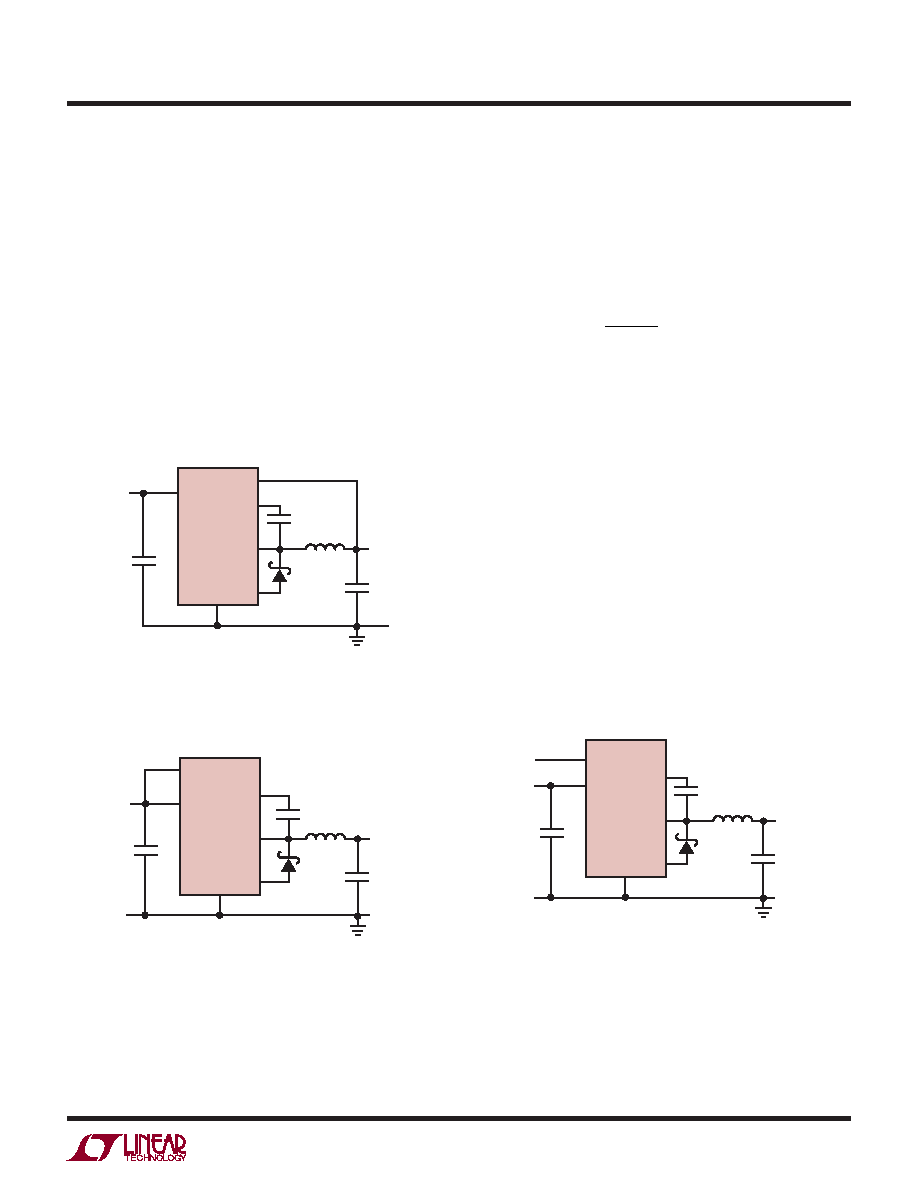
Figure 7. BD Tied to Regulated Output
L1
D1
COUT
VOUT
CBOOST
VBOOST –VSW VOUT
MAX VBOOST VIN VOUT
VOUT 3V
VIN
3509 F07
LT3509
GND
VIN
BD
BOOST
SW
DA
CIN
Boost Pin Considerations
Figure 7 through Figure 9 show several ways to arrange
the boost circuit. The BOOST pin must be more than 2V
above the SW pin for full efciency. For outputs of 3.3V
and higher, the standard circuit Figure 7 is best. For lower
output voltages, the boost diode can be tied to the input
Figure 8. The circuit in Figure 7 is more efcient because
the boost pin current comes from a lower voltage source.
Finally, as shown in Figure 9, the BD pin can be tied to
another source that is at least 3V. For example, if you are
generating 3.3V and 1.8V, and the 3.3V is on whenever
the 1.8V is on, the 1.8V boost diode can be connected to
the 3.3V output.
In any case, be sure that the maximum voltage at the
BOOST pin is less than 60V and the voltage difference
between the BOOST and SW pins is less than 30V.
Inductor Selection and Maximum Output Current
A good rst choice for the inductor value is:
LV
V
MHz
f
OUT
F
SW
=+
()
.
21
where VF is the voltage drop of the catch diode (~0.5V)
and L is in μH.
The inductor’s RMS current rating must be greater than the
maximum load current and its saturation current should
be at least 30% higher. For highest efciency, the series
resistance (DCR) should be less than 0.15Ω. Table 2 lists
several vendors and types that are suitable.
The current in the inductor is a triangle wave with an average
value equal to the load current. The peak switch current
is equal to the output current plus half the peak-to-peak
inductor ripple current. The LT3509 limits its switch current
in order to protect itself and the system from overcurrent
faults. Therefore, the maximum output current that the
LT3509 will deliver depends on the switch current limit,
the inductor value and the input and output voltages.
L1
D1
COUT
VOUT
CBOOST
VBOOST –VSW VIN
MAX VBOOST 2VIN
CIN
VIN
3509 F08
LT3509
GND
VIN
BD
BOOST
SW
DA
Figure 8. Supplied from VIN
L1
D1
COUT
VOUT
CBOOST
VBOOST –VSW VBD
MAX VBOOST VIN VBD
VBD 3V
CIN
VIN
VBD
3509 F09
LT3509
GND
VIN
BD
BOOST
SW
DA
Figure 9. Separate Boost Supply
相关PDF资料 |
PDF描述 |
|---|---|
| LT3509IMSE#PBF | 1.2 A DUAL SWITCHING CONTROLLER, 2500 kHz SWITCHING FREQ-MAX, PDSO16 |
| LT3509IMSE#TRPBF | 1.2 A DUAL SWITCHING CONTROLLER, 2500 kHz SWITCHING FREQ-MAX, PDSO16 |
| LT3509EMSE#TRPBF | 1.2 A DUAL SWITCHING CONTROLLER, 2500 kHz SWITCHING FREQ-MAX, PDSO16 |
| LT3509IDE#TRPBF | 1.2 A DUAL SWITCHING CONTROLLER, 2500 kHz SWITCHING FREQ-MAX, PDSO14 |
| LT3509IDE#PBF | 1.2 A DUAL SWITCHING CONTROLLER, 2500 kHz SWITCHING FREQ-MAX, PDSO14 |
相关代理商/技术参数 |
参数描述 |
|---|---|
| LT3509IDE#PBF | 功能描述:IC REG BUCK ADJ 0.7A DL 14DFN RoHS:是 类别:集成电路 (IC) >> PMIC - 稳压器 - DC DC 开关稳压器 系列:- 标准包装:250 系列:- 类型:降压(降压) 输出类型:固定 输出数:1 输出电压:1.2V 输入电压:2.05 V ~ 6 V PWM 型:电压模式 频率 - 开关:2MHz 电流 - 输出:500mA 同步整流器:是 工作温度:-40°C ~ 85°C 安装类型:表面贴装 封装/外壳:6-UFDFN 包装:带卷 (TR) 供应商设备封装:6-SON(1.45x1) 产品目录页面:1032 (CN2011-ZH PDF) 其它名称:296-25628-2 |
| LT3509IDE#PBF | 制造商:Linear Technology 功能描述:DC-DC CONVERTER BUCK 2.2MHZ 制造商:Linear Technology 功能描述:DC-DC CONVERTER, BUCK, 2.2MHZ, DFN-14 |
| LT3509IDE#TRPBF | 功能描述:IC REG BUCK ADJ 0.7A DL 14DFN RoHS:是 类别:集成电路 (IC) >> PMIC - 稳压器 - DC DC 开关稳压器 系列:- 标准包装:2,500 系列:- 类型:降压(降压) 输出类型:固定 输出数:1 输出电压:1.2V,1.5V,1.8V,2.5V 输入电压:2.7 V ~ 20 V PWM 型:- 频率 - 开关:- 电流 - 输出:50mA 同步整流器:是 工作温度:-40°C ~ 125°C 安装类型:表面贴装 封装/外壳:10-TFSOP,10-MSOP(0.118",3.00mm 宽)裸露焊盘 包装:带卷 (TR) 供应商设备封装:10-MSOP 裸露焊盘 |
| LT3509IDE-PBF | 制造商:LINER 制造商全称:Linear Technology 功能描述:Dual 36V, 700mA Step-Down Regulator |
| LT3509IDE-TRPBF | 制造商:LINER 制造商全称:Linear Technology 功能描述:Dual 36V, 700mA Step-Down Regulator |
发布紧急采购,3分钟左右您将得到回复。