- 您现在的位置:买卖IC网 > PDF目录1825 > LT3511MPMS#PBF (Linear Technology)IC REG FLYBK ISO ADJ .24A 16MSOP PDF资料下载
参数资料
| 型号: | LT3511MPMS#PBF |
| 厂商: | Linear Technology |
| 文件页数: | 12/26页 |
| 文件大小: | 0K |
| 描述: | IC REG FLYBK ISO ADJ .24A 16MSOP |
| 标准包装: | 37 |
| 类型: | 回扫,隔离 |
| 输出类型: | 可调式 |
| 输出数: | 1 |
| 输出电压: | 可调至 150V |
| 输入电压: | 4.5 V ~ 100 V |
| PWM 型: | 电流模式,混合 |
| 频率 - 开关: | 40kHz ~ 650kHz |
| 电流 - 输出: | 240mA |
| 同步整流器: | 无 |
| 工作温度: | -55°C ~ 150°C |
| 安装类型: | 表面贴装 |
| 封装/外壳: | 16-TFSOP(0.118",3.00mm),12 引线 |
| 包装: | 管件 |
| 供应商设备封装: | 16-MSOP |
�� �
�
�LT3511�
�APPLICATIONS� INFORMATION�
�V� SW�
�<150V�
�<100V�
�V� LEAKAGE�
�t� OFF� >� 400ns�
�V� SW�
�<150V�
�<140V�
�<100V�
�t� OFF� >� 400ns�
�t� SP� <� 150ns�
�TIME�
�t� SP� <� 150ns�
�3511� F05�
�TIME�
�without� Clamp�
�with� Clamp�
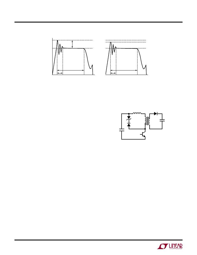
�Figure� 5.� Maximum� Voltages� for� SW� Pin� Flyback� Waveform�
�L� S�
�Leakage� Inductance� and� Clamp� Circuits�
�Z�
�Transformer� leakage� inductance� (on� either� the� primary� or�
�secondary)� causes� a� voltage� spike� to� appear� at� the� primary�
�after� the� output� switch� turns� off.� This� spike� is� increasingly�
�prominent� at� higher� load� currents� where� more� stored� en-�
�ergy� must� be� dissipated.� When� designing� an� application,�
�adequate� margin� should� be� kept� for� the� effect� of� leakage�
�voltage� spikes.� In� most� cases� the� reflected� output� voltage�
�on� the� primary� plus� V� IN� should� be� kept� below� 100V.� This�
�leaves� at� least� 50V� of� margin� for� the� leakage� spike� across�
�line� and� load� conditions.� A� larger� voltage� margin� will� be�
�needed� for� poorly� wound� transformers� or� for� excessive�
�leakage� inductance.� Figure� 5� illustrates� this� point.� Minimize�
�transformer� leakage� inductance.�
�A� clamp� circuit� is� recommended� for� most� applications.�
�Two� circuits� that� can� protect� the� internal� power� switch�
�include� the� RCD� (resistor-capacitor-diode)� clamp� and� the�
�DZ� (diode-Zener)� clamp.� The� clamp� circuits� dissipate� the�
�stored� energy� in� the� leakage� inductance.� The� DZ� clamp�
�is� the� recommended� clamp� for� the� LT3511.� Simplicity� of�
�design,� high� clamp� voltages,� and� low� power� levels� make� the�
�DZ� clamp� the� preferred� solution.� Additionally,� a� DZ� clamp�
�ensures� well� defined� and� consistent� clamping� voltages.�
�Figure� 5� shows� the� clamp� effect� on� the� switch� waveform�
�and� Figure� 6� shows� the� connection� of� the� DZ� clamp.�
�D�
�3511� F06�
�Figure� 6.� DZ� Clamp�
�Proper� care� must� be� taken� when� choosing� both� the� diode�
�and� the� Zener� diode.� Schottky� diodes� are� typically� the� best�
�choice,� but� some� PN� diodes� can� be� used� if� they� turn� on�
�fast� enough� to� limit� the� leakage� inductance� spike.� Choose�
�a� diode� that� has� a� reverse-voltage� rating� higher� than� the�
�maximum� switch� voltage.� The� Zener� diode� breakdown�
�voltage� should� be� chosen� to� balance� power� loss� and� switch�
�voltage� protection.� The� best� compromise� is� to� choose� the�
�largest� voltage� breakdown.� Use� the� following� equation� to�
�make� the� proper� choice:�
�V� ZENER(MAX)� ≤� 150V� –� V� IN(MAX)�
�For� an� application� with� a� maximum� input� voltage� of� 72V,�
�choose� a� 68V� V� ZENER� which� has� V� ZENER(MAX)� at� 72V,� which�
�will� be� below� the� 78V� maximum.�
�The� power� loss� in� the� clamp� will� determine� the� power� rat-�
�ing� of� the� Zener� diode.� Power� loss� in� the� clamp� is� highest�
�3511fc�
�12�
�相关PDF资料 |
PDF描述 |
|---|---|
| LT3512MPMS#TRPBF | IC REG FLYBK ISO ADJ .42A 16MSOP |
| LT3513IUHF#PBF | IC REG 5-OUT FOR TFT-LCD 38QFN |
| LT3571IUD#TRPBF | IC REG BOOST ADJ 0.47A 16QFN |
| LT3573IMSE#TRPBF | IC REG FLYBACK ISO ADJ 16MSOP |
| LT3574IMS#TRPBF | IC REG FLYBK ISO ADJ .65A 16MSOP |
相关代理商/技术参数 |
参数描述 |
|---|---|
| LT3512 | 制造商:LINER 制造商全称:Linear Technology 功能描述:Monolithic High Voltage Isolated Flyback Converter |
| LT3512_11 | 制造商:LINER 制造商全称:Linear Technology 功能描述:Monolithic High Voltage Isolated Flyback Converter |
| LT3512EMS#PBF | 功能描述:IC REG FLYBK ISO ADJ .42A 16MSOP RoHS:是 类别:集成电路 (IC) >> PMIC - 稳压器 - DC DC 开关稳压器 系列:- 标准包装:250 系列:- 类型:降压(降压) 输出类型:固定 输出数:1 输出电压:1.2V 输入电压:2.05 V ~ 6 V PWM 型:电压模式 频率 - 开关:2MHz 电流 - 输出:500mA 同步整流器:是 工作温度:-40°C ~ 85°C 安装类型:表面贴装 封装/外壳:6-UFDFN 包装:带卷 (TR) 供应商设备封装:6-SON(1.45x1) 产品目录页面:1032 (CN2011-ZH PDF) 其它名称:296-25628-2 |
| LT3512EMS#TRPBF | 功能描述:IC REG FLYBK ISO ADJ .42A 16MSOP RoHS:是 类别:集成电路 (IC) >> PMIC - 稳压器 - DC DC 开关稳压器 系列:- 标准包装:2,500 系列:- 类型:降压(降压) 输出类型:固定 输出数:1 输出电压:1.2V,1.5V,1.8V,2.5V 输入电压:2.7 V ~ 20 V PWM 型:- 频率 - 开关:- 电流 - 输出:50mA 同步整流器:是 工作温度:-40°C ~ 125°C 安装类型:表面贴装 封装/外壳:10-TFSOP,10-MSOP(0.118",3.00mm 宽)裸露焊盘 包装:带卷 (TR) 供应商设备封装:10-MSOP 裸露焊盘 |
| LT3512EMSPBF | 制造商:LINER 制造商全称:Linear Technology 功能描述:Monolithic High Voltage Isolated Flyback Converter |
发布紧急采购,3分钟左右您将得到回复。