- 您现在的位置:买卖IC网 > PDF目录14810 > LT3512EMS#PBF (Linear Technology)IC REG FLYBK ISO ADJ .42A 16MSOP PDF资料下载
参数资料
| 型号: | LT3512EMS#PBF |
| 厂商: | Linear Technology |
| 文件页数: | 15/26页 |
| 文件大小: | 0K |
| 描述: | IC REG FLYBK ISO ADJ .42A 16MSOP |
| 标准包装: | 37 |
| 类型: | 回扫,隔离 |
| 输出类型: | 可调式 |
| 输出数: | 1 |
| 输出电压: | 可调 |
| 输入电压: | 4.5 V ~ 100 V |
| PWM 型: | 电流模式,混合 |
| 频率 - 开关: | 40kHz ~ 650kHz |
| 电流 - 输出: | 420mA |
| 同步整流器: | 无 |
| 工作温度: | -40°C ~ 125°C |
| 安装类型: | 表面贴装 |
| 封装/外壳: | 16-TFSOP(0.118",3.00mm),12 引线 |
| 包装: | 管件 |
| 供应商设备封装: | 16-MSOP |
�� �
�
�LT3512�
�APPLICATIONS� INFORMATION�
�order� to� regulate� the� output� voltage,� the� LT3512� needs� to�
�sample� the� flyback� pulse.� The� LT3512� delivers� a� minimum�
�amount� of� energy� even� during� light� load� conditions� to�
�ensure� accurate� output� voltage� information.� The� minimum�
�delivery� of� energy� creates� a� minimum� load� requirement�
�of� 20mA� to� 25mA� depending� on� the� specific� application.�
�Verify� minimum� load� requirements� for� each� application.�
�A� Zener� diode� with� a� Zener� breakdown� of� 20%� higher�
�than� the� output� voltage� can� serve� as� a� minimum� load� if�
�pre-loading� is� not� acceptable.� For� a� 5V� output,� use� a� 6V�
�Zener� with� cathode� connected� to� the� output.�
�LT3512�
�LT3512�
�V� IN�
�LDO�
�BIAS�
�V� IN�
�LDO�
�6V� TO� 100V�
�3V�
�4.5V� TO� 15V�
�V� IN�
�EXTERNAL�
�BIAS�
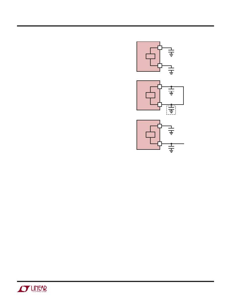
�BIASPinConsiderations�
�The� BIAS� pin� powers� the� internal� circuitry� of� the� LT3512.�
�Three� unique� configurations� exist� for� regulation� of� the� BIAS�
�pin.� In� the� first� configuration,� the� internal� LDO� drives� the�
�BIAS� pin� internally� from� the� V� IN� supply.� In� the� second� setup,�
�the� V� IN� supply� directly� drives� the� BIAS� pin� through� a� direct�
�connection� bypassing� the� internal� LDO.� This� configuration�
�will� allow� the� part� to� operate� down� to� 4.5V� and� up� to� 15V.�
�In� the� third� configuration,� an� external� supply� or� third� wind-�
�ing� drives� the� BIAS� pin.� Use� this� option� when� a� voltage�
�supply� exists� lower� than� the� input� supply.� Drive� the� BIAS�
�pin� with� a� voltage� supply� higher� than� 3.3V� to� disable� the�
�internal� LDO.� The� lower� voltage� supply� provides� a� more�
�efficient� source� of� power� for� internal� circuitry.�
�Overdriving� the� BIAS� Pin� with� a� Third� Winding�
�The� LT3512� provides� excellent� output� voltage� regulation�
�without� the� need� for� an� opto-coupler,� or� third� winding,�
�but� for� some� applications� with� higher� input� voltages�
�(>20V),� an� additional� winding� (often� called� a� third� winding)�
�improves� overall� system� efficiency.� Design� the� third� wind-�
�ing� to� output� a� voltage� between� 3.3V� and� 12V.� For� a� typi-�
�cal� 48V� IN� application,� overdriving� the� BIAS� pin� improves�
�efficiency� 4%� to� 5%.�
�Loop� Compensation�
�An� external� resistor-capacitor� network� compensates� the�
�LT3512� on� the� VC� pin.� Typical� compensation� values� are� in�
�the� range� of� R� C� =� 15k� and� C� C� =� 4.7nF� (see� the� numerous�
�schematics� in� the� Typical� Applications� section� for� other� pos-�
�sible� values).� Proper� choice� of� both� R� C� and� C� C� is� important�
�to� achieve� stability� and� acceptable� transient� response.� For�
�BIAS�
�OPTIONAL�
�LT3512� 6V� TO� 100V�
�LDO�
�3.3V� <� BIAS� <� 20V�
�SUPPLY�
�3512� F08�
�Figure� 8.� BIAS� Pin� Configurations�
�example,� vulnerability� to� high� frequency� noise� and� jitter�
�result� when� R� C� is� too� large.� On� the� other� hand,� if� R� C� is�
�too� small,� transient� performance� suffers.� The� inverse� is�
�true� with� respect� to� the� value� of� C� C� .� Transient� response�
�suffers� with� too� large� of� a� C� C� ,� and� instability� results� from�
�too� small� a� C� C� .� The� specific� value� for� R� C� and� C� C� will� vary�
�based� on� the� application� and� transformer� choice.� Verify�
�specific� choices� with� board� level� evaluation� and� transient�
�response� performance.�
�DESIGN� PROCEDURE/DESIGN� EXAMPLE�
�Use� the� following� design� procedure� as� a� guide� to� design-�
�ing� applications� for� the� LT3512.� Remember,� the� unique�
�sampling� architecture� requires� an� iterative� process� for�
�choosing� correct� resistor� values.�
�The� design� example� involves� designing� a� 15V� output� with�
�a� 200mA� load� current� and� an� input� range� from� 36V� to� 72V.�
�V� IN(MIN)� =� 36V,� V� IN(NOM)� =� 48V,� V� IN(MAX)� =� 72V,� V� OUT� =�
�15V� and� I� OUT� =� 200mA�
�3512fb�
�15�
�相关PDF资料 |
PDF描述 |
|---|---|
| LT3508EUF#PBF | IC REG BUCK ADJ 1.4A DL 24QFN |
| RYM22DRMH | CONN EDGECARD 44POS .156 WW |
| LT1372CN8#PBF | IC REG MULTI CONFIG ADJ 8DIP |
| LTC1174CN8#PBF | IC REG BUCK INV ADJ 1A 8DIP |
| LTC1875EGN#PBF | IC REG BUCK SYNC ADJ 1.5A 16SSOP |
相关代理商/技术参数 |
参数描述 |
|---|---|
| LT3512HMS#PBF | 功能描述:IC REG FLYBK ISO ADJ .42A 16MSOP RoHS:是 类别:集成电路 (IC) >> PMIC - 稳压器 - DC DC 开关稳压器 系列:- 设计资源:Design Support Tool 标准包装:1 系列:- 类型:升压(升压) 输出类型:固定 输出数:1 输出电压:3V 输入电压:0.75 V ~ 2 V PWM 型:- 频率 - 开关:- 电流 - 输出:100mA 同步整流器:是 工作温度:-40°C ~ 85°C 安装类型:表面贴装 封装/外壳:SOT-23-5 细型,TSOT-23-5 包装:剪切带 (CT) 供应商设备封装:TSOT-23-5 其它名称:AS1323-BTTT-30CT |
| LT3512HMS#TRPBF | 功能描述:IC REG FLYBK ISO ADJ .42A 16MSOP RoHS:是 类别:集成电路 (IC) >> PMIC - 稳压器 - DC DC 开关稳压器 系列:- 设计资源:Design Support Tool 标准包装:1 系列:- 类型:升压(升压) 输出类型:固定 输出数:1 输出电压:3V 输入电压:0.75 V ~ 2 V PWM 型:- 频率 - 开关:- 电流 - 输出:100mA 同步整流器:是 工作温度:-40°C ~ 85°C 安装类型:表面贴装 封装/外壳:SOT-23-5 细型,TSOT-23-5 包装:剪切带 (CT) 供应商设备封装:TSOT-23-5 其它名称:AS1323-BTTT-30CT |
| LT3512HMSPBF | 制造商:LINER 制造商全称:Linear Technology 功能描述:Monolithic High Voltage Isolated Flyback Converter |
| LT3512IMS#PBF | 功能描述:IC REG FLYBK ISO ADJ .42A 16MSOP RoHS:是 类别:集成电路 (IC) >> PMIC - 稳压器 - DC DC 开关稳压器 系列:- 标准包装:2,500 系列:- 类型:降压(降压) 输出类型:固定 输出数:1 输出电压:1.2V,1.5V,1.8V,2.5V 输入电压:2.7 V ~ 20 V PWM 型:- 频率 - 开关:- 电流 - 输出:50mA 同步整流器:是 工作温度:-40°C ~ 125°C 安装类型:表面贴装 封装/外壳:10-TFSOP,10-MSOP(0.118",3.00mm 宽)裸露焊盘 包装:带卷 (TR) 供应商设备封装:10-MSOP 裸露焊盘 |
| LT3512IMS#TRPBF | 功能描述:IC REG FLYBK ISO ADJ .42A 16MSOP RoHS:是 类别:集成电路 (IC) >> PMIC - 稳压器 - DC DC 开关稳压器 系列:- 设计资源:Design Support Tool 标准包装:1 系列:- 类型:升压(升压) 输出类型:固定 输出数:1 输出电压:3V 输入电压:0.75 V ~ 2 V PWM 型:- 频率 - 开关:- 电流 - 输出:100mA 同步整流器:是 工作温度:-40°C ~ 85°C 安装类型:表面贴装 封装/外壳:SOT-23-5 细型,TSOT-23-5 包装:剪切带 (CT) 供应商设备封装:TSOT-23-5 其它名称:AS1323-BTTT-30CT |
发布紧急采购,3分钟左右您将得到回复。