- 您现在的位置:买卖IC网 > PDF目录14112 > LT3580EDD#TRPBF (Linear Technology)IC REG BOOST INV SEPIC 2A 8DFN PDF资料下载
参数资料
| 型号: | LT3580EDD#TRPBF |
| 厂商: | Linear Technology |
| 文件页数: | 5/28页 |
| 文件大小: | 0K |
| 描述: | IC REG BOOST INV SEPIC 2A 8DFN |
| 标准包装: | 2,500 |
| 类型: | 升压(升压),反相,Sepic |
| 输出数: | 1 |
| 输入电压: | 2.5 V ~ 32 V |
| PWM 型: | 电流模式 |
| 频率 - 开关: | 200kHz ~ 2.5MHz |
| 电流 - 输出: | 2A |
| 同步整流器: | 无 |
| 工作温度: | -40°C ~ 125°C |
| 安装类型: | 表面贴装 |
| 封装/外壳: | 8-WFDFN 裸露焊盘 |
| 包装: | 带卷 (TR) |
| 供应商设备封装: | 8-DFN-EP(3x3) |
第1页第2页第3页第4页当前第5页第6页第7页第8页第9页第10页第11页第12页第13页第14页第15页第16页第17页第18页第19页第20页第21页第22页第23页第24页第25页第26页第27页第28页
�� �
�
�LT3580�
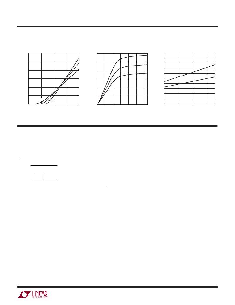
�TYPICAL� PERFORMANCE� CHARACTERISTICS�
�T� A� =� 25°C� unless� otherwise� specified�
�30�
�SHDN� Pin� Current�
�300�
�SHDN� Pin� Current�
�–50°C�
�1.40�
�1.38�
�Active/Lockout� Threshold�
�25�
�250�
�20°C�
�1.36�
�20�
�15�
�10�
�5�
�–50°C�
�200�
�150�
�100�
�50�
�100°C�
�1.34�
�1.32�
�1.30�
�1.28�
�1.26�
�1.24�
�SHDN� RISING�
�SHDN� FALLING�
�0�
�0�
�100°C�
�0.5�
�20°C�
�1�
�1.5�
�2�
�0�
�0�
�5�
�10�
�15�
�20�
�25�
�30�
�1.22�
�1.20�
�–50�
�0�
�50�
�100�
�SHDN� VOLTAGE� (V)�
�PIN� FUNCTIONS�
�3580� G10�
�SHDN� VOLTAGE� (V)�
�3580� G11�
�TEMPERATURE� (°C)�
�3580� G12�
�FB� (Pin� 1):� Positive� and� Negative� Feedback� Pin.� For� a�
�boost� or� inverting� converter,� tie� a� resistor� from� the� FB� pin�
�to� V� OUT� according� to� the� following� equations:�
�RT� (Pin� 6):� Timing� Resistor� Pin.� Adjusts� the� switching�
�frequency.� Place� a� resistor� from� this� pin� to� ground� to� set�
�the� frequency� to� a� fixed� free� running� level.� Do� not� float�
�R� FB� =�
�R� FB� =�
�(� V� OUT� ?� 1.215� )� ;� Boost� or� SEPIC� Converter�
�83.3� ?� 10� ?� 6�
�(� V� OUT� +� 5mV� )� ;� Inverting� Converter�
�83.3� ?� 10� ?� 6�
�this� pin.�
�SS� (Pin� 7):� Soft-Start� Pin.� Place� a� soft-start� capacitor� here.�
�Upon� start-up,� the� SS� pin� will� be� charged� by� a� (nominally)�
�275k� resistor� to� about� 2.2V.�
�SYNC� (Pin� 8):� To� synchronize� the� switching� frequency� to�
�VC� (Pin� 2):� Error� Amplifier� Output� Pin.� Tie� external�
�compensation� network� to� this� pin.�
�V� IN� (Pin� 3):� Input� Supply� Pin.� Must� be� locally� bypassed.�
�SW� (Pin� 4):� Switch� Pin.� This� is� the� collector� of� the� internal�
�NPN� Power� switch.� Minimize� the� metal� trace� area� connec-�
�ted� to� this� pin� to� minimize� EMI.�
�an� outside� clock,� simply� drive� this� pin� with� a� clock.� The�
�high� voltage� level� of� the� clock� needs� to� exceed� 1.3V,� and�
�the� low� level� should� be� less� 0.4V.� Drive� this� pin� to� less� than�
�0.4V� to� revert� to� the� internal� free� running� clock.� See� the�
�Applications� Information� section� for� more� information.�
�GND� (Exposed� Pad� Pin� 9):� Ground.� Exposed� pad� must�
�be� soldered� directly� to� local� ground� plane.�
�SHDN� (Pin� 5):� Shutdown� Pin.� In� conjunction� with� the�
�UVLO� (undervoltage� lockout)� circuit,� this� pin� is� used�
�to� enable/disable� the� chip� and� restart� the� soft-start�
�sequence.� Drive� below� 1.24V� (LT3580E,� LT3580I)� or� 1.22V�
�(LT3580H,� LT3580MP)� to� disable� the� chip.� Drive� above�
�1.38V� (LT3580E,� LT3580I)� or� 1.40V� (LT3580H,� LT3580MP)�
�to� activate� chip� and� restart� the� soft-start� sequence.� Do�
�not� float� this� pin.�
�3580fg�
�5�
�相关PDF资料 |
PDF描述 |
|---|---|
| RCB40DHNT | CONN EDGECARD 80POS DIP .050 SLD |
| LNX2V123MSEH | CAP ALUM 12000UF 350V 20% SCREW |
| CGS432T400W5L | CAP ALUM 4300UF 400V SCREW |
| RCB40DHHT | CONN EDGECARD 80POS DIP .050 SLD |
| RBB13DHAT | CONN EDGECARD 26POS R/A .050 DIP |
相关代理商/技术参数 |
参数描述 |
|---|---|
| LT3580EMS8E | 制造商:LINER 制造商全称:Linear Technology 功能描述:Boost/Inverting DC/DC Converter with 2A Switch, Soft-Start, and Synchronization |
| LT3580EMS8E#PBF | 功能描述:IC REG BOOST INV SEPIC 2A 8MSOP RoHS:是 类别:集成电路 (IC) >> PMIC - 稳压器 - DC DC 开关稳压器 系列:- 标准包装:250 系列:- 类型:降压(降压) 输出类型:固定 输出数:1 输出电压:1.2V 输入电压:2.05 V ~ 6 V PWM 型:电压模式 频率 - 开关:2MHz 电流 - 输出:500mA 同步整流器:是 工作温度:-40°C ~ 85°C 安装类型:表面贴装 封装/外壳:6-UFDFN 包装:带卷 (TR) 供应商设备封装:6-SON(1.45x1) 产品目录页面:1032 (CN2011-ZH PDF) 其它名称:296-25628-2 |
| LT3580EMS8E#PBF | 制造商:Linear Technology 功能描述:Switching Regulator IC 制造商:Linear Technology 功能描述:IC BOOST/INVERTING DC/DC CONVERTER MSOP8 |
| LT3580EMS8E#TRPBF | 功能描述:IC REG BOOST INV SEPIC 2A 8MSOP RoHS:是 类别:集成电路 (IC) >> PMIC - 稳压器 - DC DC 开关稳压器 系列:- 标准包装:2,500 系列:- 类型:升压(升压) 输出类型:可调式 输出数:1 输出电压:1.24 V ~ 30 V 输入电压:1.5 V ~ 12 V PWM 型:电流模式,混合 频率 - 开关:600kHz 电流 - 输出:500mA 同步整流器:无 工作温度:-40°C ~ 85°C 安装类型:表面贴装 封装/外壳:8-SOIC(0.154",3.90mm 宽) 包装:带卷 (TR) 供应商设备封装:8-SOIC |
| LT3580EMS8EPBF | 制造商:Linear Technology 功能描述:2A Boost/Inverting switch,sync LT3580 |
发布紧急采购,3分钟左右您将得到回复。