- 您现在的位置:买卖IC网 > PDF目录1825 > LT3581IMSE#TRPBF (Linear Technology)IC REG MULTI CONFIG ADJ 16MSOP PDF资料下载
参数资料
| 型号: | LT3581IMSE#TRPBF |
| 厂商: | Linear Technology |
| 文件页数: | 13/36页 |
| 文件大小: | 0K |
| 描述: | IC REG MULTI CONFIG ADJ 16MSOP |
| 标准包装: | 2,500 |
| 类型: | 升压(升压),反相,回扫,Sepic |
| 输出类型: | 可调式 |
| 输出数: | 1 |
| 输出电压: | 1.22 V ~ 42 V |
| 输入电压: | 2.5 V ~ 22 V |
| PWM 型: | 电流模式 |
| 频率 - 开关: | 200kHz ~ 2.5MHz |
| 电流 - 输出: | 3.3A |
| 同步整流器: | 无 |
| 工作温度: | -40°C ~ 125°C |
| 安装类型: | 表面贴装 |
| 封装/外壳: | 16-TFSOP(0.118",3.00mm 宽)裸露焊盘 |
| 包装: | 带卷 (TR) |
| 供应商设备封装: | 16-MSOP,裸露焊盘 |
第1页第2页第3页第4页第5页第6页第7页第8页第9页第10页第11页第12页当前第13页第14页第15页第16页第17页第18页第19页第20页第21页第22页第23页第24页第25页第26页第27页第28页第29页第30页第31页第32页第33页第34页第35页第36页
�� �
�
�LT3581�
�APPLICATIONS� INFORMATION�
�L1�
�1.5μH�
�V� OUT�
�V� IN�
�5V�
�R� GATE�
�SW1� SW2�
�C� IN�
�R� FAULT� LT3581� R� FB�
�130k�
�C� OUT2�
�R� C�
�10.5k�
�SYNC�
�SS�
�C� SS�
�R� T�
�C� C�
�43.2k�
�1nF�
�Step� 2:� V� OUT� –� V� IN� +� 0� .� 5� V�
�V� OUT� +� 0� .� 5� V� –� 0� .� 3� V�
�(� V� IN� –� 0� .� 3� V� )� ?� DC�
�L� TYP� =�
�(� V� IN� –� 0� .� 3� V� )� ?� (� 2� ?� D� C� –� 1� )�
�2� .� 2� A� ?� f� OSC� ?� (� 1� –� DC� )�
�(� V� IN� –� 0� .� 3� V� )� ?� DC�
�=�
�L� MAX�
�L1�
�f� O� S� C� ?� 0� .� 35� A�
�Step� 4:� (� V� IN� –� 0� .� 3� V� )� ?� DC�
�I� RIPPLE� =�
�I� OUT� =� ?� 3� .� 3� A� –� RIPPLE� ?� ?� (� 1� –� DC� )�
�?� I� ?�
�V� R� >� V� OUT� ;� I� AVG� >� I� OUT�
�BOOST� CONVERTER� COMPONENT� SELECTION�
�D1� OPTIONAL�
�20V,� 2A�
�PMOS�
�12V�
�C� OUT1� I� OUT� <� 0.83A�
�4.7μF�
�6.04k�
�V� IN� FB�
�4.7μF� 100k�
�FAULT� GATE�
�SHDN� CLKOUT� 4.7μF�
�RT� V� C�
�C� F�
�56pF�
�GND�
�0.1μF�
�3581� F05�
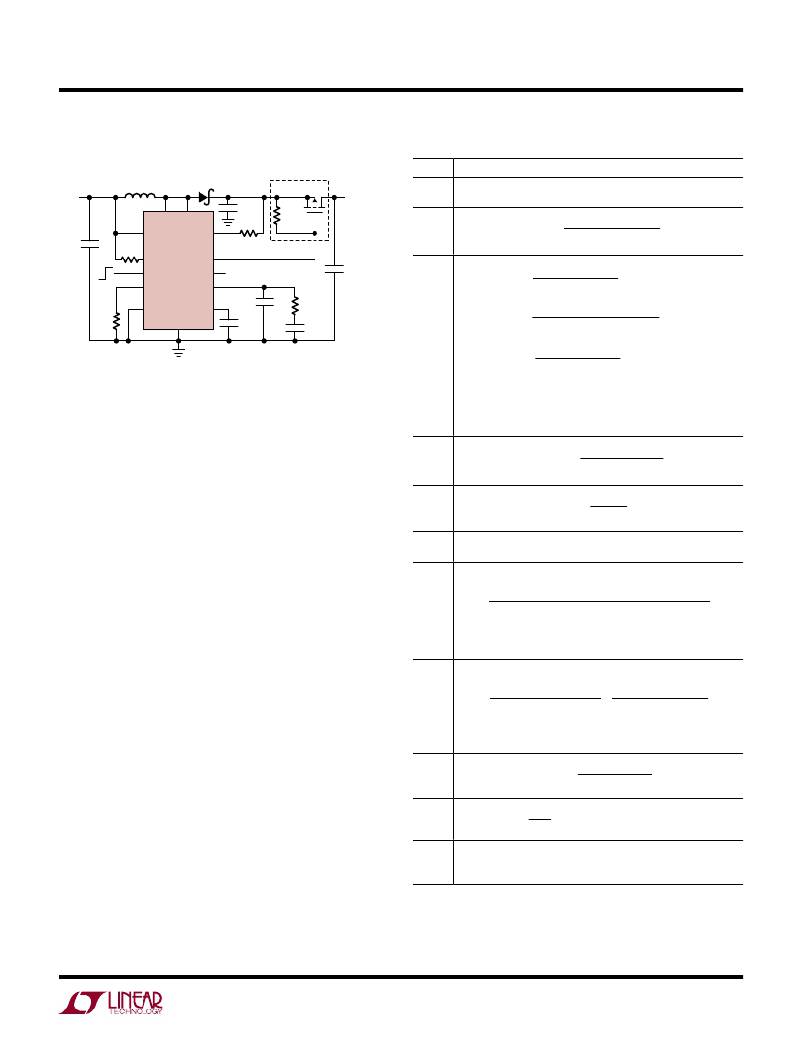
�Figure� 5.� Boost� Converter� –� The� Component� Values� and� Voltages�
�Given� Are� Typical� Values� for� a� 2MHz,� 5V� to� 12V� Boost�
�The� LT3581� can� be� configured� as� a� Boost� converter� as�
�in� Figure� 5.� This� topology� allows� for� positive� output� volt-�
�ages� that� are� higher� than� the� input� voltage.� An� external�
�PMOS� (optional)� driven� by� the� GATE� pin� of� the� LT3581� can�
�achieve� input� or� output� disconnect� during� a� fault� event.�
�A� single� feedback� resistor� sets� the� output� voltage.� For�
�output� voltages� higher� than� 40V,� see� the� Charge� Pump�
�Aided� Regulators� section.�
�Table 1.� Boost� Design� Equations�
�PARAMETERS/EQUATIONS�
�Step� 1:� Pick� V� IN� ,� V� OUT� ,� and� f� OSC� to� calculate� equations� below.�
�Inputs�
�DC� ?�
�DC�
�(1)�
�f� OSC� ?� 1� A�
�L� MIN� =� (2)�
�Step� 3:�
�(3)�
�?� Pick� L1� out� of� a� range� of� inductor� values� where� the� minimum�
�value� of� the� range� is� set� by� L� TYP� or� L� MIN� ,� whichever� is� higher.�
�The� maximum� value� of� the� range� is� set� by� L� MAX� .� See� appendix�
�on� how� to� choose� current� rating� for� inductor� value� chosen.�
�I� RIPPLE� f� OSC� ?� L� 1�
�Step� 5:�
�I� OUT� ?� 2� ?�
�Step� 6:�
�D1�
�+�
�R� FB� =�
�R� T� =�
�–� 1� ;� f� OSC� in� MHz� and� R� T� in� k� ?�
�Table� 1� is� a� step-by-step� set� of� equations� to� calculate�
�component� values� for� the� LT3581� when� operating� as� a�
�boost� converter.� Input� parameters� are� input� and� output�
�voltage,� and� switching� frequency� (V� IN� ,� V� OUT� and� f� OSC� re-�
�spectively).� Refer� to� the� Appendix� for� further� information�
�on� the� design� equations� presented� in� Table� 1.�
�Variable� Definitions:�
�V� IN� =� Input� Voltage�
�V� OUT� =� Output� Voltage�
�DC� =� Power� Switch� Duty� Cycle�
�f� OSC� =� Switching� Frequency�
�I� OUT� =� Maximum� Average� Output� Current�
�I� RIPPLE� =� Inductor� Ripple� Current�
�R� DSON_PMOS� =� R� DSON� of� External� PMOS� (set� to� 0� if� not�
�using� PMOS)�
�Step� 7:�
�C� OUT1� ,�
�C� OUT2�
�Step� 8:�
�C� IN�
�Step� 9:�
�R� FB�
�Step� 10:�
�R� T�
�Step� 11:�
�PMOS�
�C� OUT� 1� =� C� OUT� 2� ≥�
�I� OUT� ?� DC�
�f� OSC� ??� 0� .� 01� ?� V� OUT� –� 0� .� 50� ?� I� OUT� ?� R� DSON� _� PMOS� ??�
�?� If� PMOS� is� not� used,� then� use� just� one� capacitor� where�
�C� OUT� =� C� OUT1� +� C� OUT2� .�
�C� IN� ≥� C� VIN� +� C� PWR� ≥�
�3� .� 3� A� ?� DC� I� RIP� P� LE�
�45� ?� f� OSC� ?� 0� .� 005� ?� V� IN� 8� ?� f� OSC� ?� 0� .� 005� ?� V� IN�
�?� Refer� to� Input� Capacitor� Selection� in� Appendix� for� definition� of�
�C� VIN� and� C� PWR� .�
�V� OUT� – 1. 215 V�
�83� .� 3� μA�
�87.6�
�f� OSC�
�Only� needed� for� input� or� output� disconnect.� See� PMOS� Selection�
�in� the� Appendix� for� information� on� sizing� the� PMOS,� R� GATE� and�
�picking� appropriae� UVLO� components.�
�Note� 1:� The� maximum� design� target� for� peak� switch� current� is� 3.3A� and� is�
�used� in� this� table.�
�Note� 2:� The� final� values� for� C� OUT1� ,� C� OUT2� and� C� IN� may� deviate� from� the�
�above� equations� in� order� to� obtain� desired� load� transient� performance.�
�3581fa�
�For� more� information� www.linear.com/LT3581�
�13�
�相关PDF资料 |
PDF描述 |
|---|---|
| LT3582EUD-5#TRPBF | IC REG BOOST INV +/-5V DL 16QFN |
| LT3587EUD#TRPBF | IC REG BOOST INV ADJ DL 20QFN |
| LT3640IFE#TRPBF | IC REG BUCK FIX/ADJ DL 28TSSOP |
| LT3641HFE#TRPBF | IC REG BUCK SYNC ADJ DL 28TSSOP |
| LT3650IMSE-8.4#TRPBF | IC CHARGER LI-ION 8.4V 2A 12MSOP |
相关代理商/技术参数 |
参数描述 |
|---|---|
| LT3582 | 制造商:LINER 制造商全称:Linear Technology 功能描述:I2C Programmable Boost and Single Inductor Inverting DC/DC Converters with OTP |
| LT3582-12 | 制造商:LINER 制造商全称:Linear Technology 功能描述:I2C Programmable Boost and Single Inductor Inverting DC/DC Converters with OTP |
| LT3582-5 | 制造商:LINER 制造商全称:Linear Technology 功能描述:I2C Programmable Boost and Single Inductor Inverting DC/DC Converters with OTP |
| LT3582EUD#PBF | 功能描述:IC REG BOOST INV ADJ DL 16QFN RoHS:是 类别:集成电路 (IC) >> PMIC - 稳压器 - DC DC 开关稳压器 系列:- 标准包装:250 系列:- 类型:降压(降压) 输出类型:固定 输出数:1 输出电压:1.2V 输入电压:2.05 V ~ 6 V PWM 型:电压模式 频率 - 开关:2MHz 电流 - 输出:500mA 同步整流器:是 工作温度:-40°C ~ 85°C 安装类型:表面贴装 封装/外壳:6-UFDFN 包装:带卷 (TR) 供应商设备封装:6-SON(1.45x1) 产品目录页面:1032 (CN2011-ZH PDF) 其它名称:296-25628-2 |
| LT3582EUD#TRPBF | 功能描述:IC REG BOOST INV ADJ DL 16QFN RoHS:是 类别:集成电路 (IC) >> PMIC - 稳压器 - DC DC 开关稳压器 系列:- 标准包装:2,500 系列:- 类型:升压(升压) 输出类型:可调式 输出数:1 输出电压:1.24 V ~ 30 V 输入电压:1.5 V ~ 12 V PWM 型:电流模式,混合 频率 - 开关:600kHz 电流 - 输出:500mA 同步整流器:无 工作温度:-40°C ~ 85°C 安装类型:表面贴装 封装/外壳:8-SOIC(0.154",3.90mm 宽) 包装:带卷 (TR) 供应商设备封装:8-SOIC |
发布紧急采购,3分钟左右您将得到回复。