- 您现在的位置:买卖IC网 > PDF目录1825 > LT3582EUD-5#TRPBF (Linear Technology)IC REG BOOST INV +/-5V DL 16QFN PDF资料下载
参数资料
| 型号: | LT3582EUD-5#TRPBF |
| 厂商: | Linear Technology |
| 文件页数: | 12/28页 |
| 文件大小: | 0K |
| 描述: | IC REG BOOST INV +/-5V DL 16QFN |
| 标准包装: | 2,500 |
| 类型: | 升压(升压),反相 |
| 输出类型: | 固定 |
| 输出数: | 2 |
| 输出电压: | ±5V |
| 输入电压: | 2.55 V ~ 5.5 V |
| PWM 型: | 混合物 |
| 电流 - 输出: | 350mA,600mA |
| 同步整流器: | 无 |
| 工作温度: | -40°C ~ 125°C |
| 安装类型: | 表面贴装 |
| 封装/外壳: | 16-WFQFN 裸露焊盘 |
| 包装: | 带卷 (TR) |
| 供应商设备封装: | 16-QFN-EP(3x3) |
第1页第2页第3页第4页第5页第6页第7页第8页第9页第10页第11页当前第12页第13页第14页第15页第16页第17页第18页第19页第20页第21页第22页第23页第24页第25页第26页第27页第28页
�� �
�
�LT3582/LT3582-5/LT3582-12�
�APPLICATIONS� INFORMATION�
�All� data� bytes� can� be� read� from� their� assigned� register�
�addresses.� Since� they� share� the� same� register� addresses,�
�reads� of� the� OTP� and� REG� data� bytes� are� differentiated�
�by� their� corresponding� RSEL� (Register� Select)� bits� in� the�
�CMDR� register.� All� data� written� to� register� addresses� 0-2� is�
�stored� in� REGO-REG2.� Regardless� of� the� RSEL� bits,� OTP�
�bytes� cannot� be� written� directly.� See� the� OTP� Programming�
�section� for� more� information.�
�Data� Transfer� Protocol�
�The� LT3582� series� supports� 8-bit� data� transfers� in� the�
�transaction� formats� shown� in� Figures� 2� and� 3.� Multiple�
�data� bytes� can� only� be� transferred� by� issuing� multiple�
�transactions.�
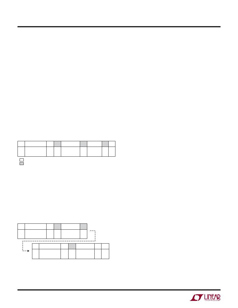
�Figure� 2� shows� the� required� format� for� writing� a� byte� of�
�data� to� the� LT3582� series.� Again,� the� chip� address� depends�
�on� the� CA� pin� logic� state.�
�LT3582� Chip� Con?guration�
�Settings� such� as� output� voltages� and� sequencing� are�
�digitally� programmable.� The� chip� uses� settings� from� either�
�the� REG� or� OTP� bytes,� depending� on� the� states� of� the�
�corresponding� RSEL� bits� (0� for� OTP� and� 1� for� REG).�
�During� shutdown� the� RSEL� bits� are� reset� low.� As� a� result,�
�the� initial� con?guration� comes� from� the� OTP� data� bytes.�
�After� power-up,� the� con?guration� can� be� changed� by� writing�
�new� settings� to� the� appropriate� REG� data� byte(s)� then�
�setting� the� corresponding� RSEL� bit(s).�
�Finally,� data� in� the� REG� bytes� can� be� permanently�
�programmed� to� OTP� by� applying� voltage� to� the� V� PP� pin�
�and� setting� the� WOTP� bit� in� the� Command� Register.� See�
�the� OTP� Programming� section� for� more� information.�
�LT3582-5/LT3582-12� Chip� Con?guration�
�S�
�CHIP� ADDR�
�W�
�A�
�REG� ADDR�
�A�
�DATA�
�A�
�P�
�The� LT3582-5/LT3582-12� are� shipped� from� the� factory� with�
�the� OTP� memory� pre-programmed� and� LOCKed� which�
�0110� 001� OR� 0� 0�
�1000� 101�
�FROM� MASTER� TO� SLAVE�
�FROM� SLAVE� TO� MASTER�
�00000b2:b0� 0� b7:b0� 0�
�A:� ACKNOWLEDGE� (LOW)�
�A� :� NOT� ACKNOWLEDGE� (HIGH)�
�R:� READ� BIT� (HIGH)�
�W� WRITE� BIT� (LOW)�
�S:� START� CONDITION�
�P:� STOP� CONDITION�
�prohibits� subsequent� changes� to� the� con?guration.� The�
�con?guration� can� still� be� read� through� the� I� 2� C� bus� and�
�the� RST� and� SWOFF� bits� of� the� CMDR� register� (described�
�later)� are� functional.� The� following� sections� describe� the�
�various� con?gurable� features� of� the� LT3582.� The� LT3582-5�
�and� LT3582-12� are� pre-con?gured� as� follows:� V� P� and� V� N�
�Figure� 2.� I� 2� C� Byte� Write� Transaction�
�A� byte� of� data� is� read� from� the� LT3582� series� using� the�
�format� shown� in� Figure� 3.� This� transaction� requires� four� I� 2� C�
�bytes� to� read� one� byte� of� chip� data� and� must� be� repeated�
�for� each� subsequent� byte� of� data� that� is� read.�
�are� programmed� for� ±5V� or� ±12V� respectively,� LOCK� =� 1,�
�IRMP� =� 00,� PDDIS� =� 1,� PUSEQ� =� 11� and� V� PLUS� may� be� 1�
�or� 0.� Since� LOCK� =� 1,� subsequent� con?guration� changes�
�are� prohibited.� See� Con?guration� Lockout� (LOCK� Bit)� for�
�more� information.�
�Registers� and� OTP�
�S�
�CHIP� ADDR�
�0110� 001� OR�
�1000� 101�
�W�
�0�
�A�
�0�
�REG� ADDR�
�00000b2:b0�
�A�
�0�
�The� registers� and� OTP� bytes� for� the� LT3582� series� are�
�organized� as� shown� in� Table� 1.� The� CMDR� is� reset� to� 00h�
�upon� power-up,� during� shutdown� and� during� undervoltage�
�and� thermal� lockouts.� REG0-REG2� are� never� reset� and� must�
�S�
�CHIP� ADDR�
�0110� 001� OR�
�1000� 101�
�R�
�1�
�A�
�0�
�DATA�
�b7:b0�
�A�
�1�
�P�
�always� be� loaded� with� valid� data� before� use.� The� LT3582’s�
�OTP� memory� is� shipped� with� all� 0’s,� and� as� a� result,� the�
�PUSEQ� bits� are� con?gured� to� disable� the� outputs.� The�
�Figure� 3.� I� 2� C� Byte� Read� Transaction�
�PUSEQ� bits� must� be� recon?gured� to� enable� the� outputs.�
�3582512fb�
�12�
�相关PDF资料 |
PDF描述 |
|---|---|
| LT3587EUD#TRPBF | IC REG BOOST INV ADJ DL 20QFN |
| LT3640IFE#TRPBF | IC REG BUCK FIX/ADJ DL 28TSSOP |
| LT3641HFE#TRPBF | IC REG BUCK SYNC ADJ DL 28TSSOP |
| LT3650IMSE-8.4#TRPBF | IC CHARGER LI-ION 8.4V 2A 12MSOP |
| LT3652EMSE#PBF | IC BATTERY CHARGER SOLAR 12MSOP |
相关代理商/技术参数 |
参数描述 |
|---|---|
| LT3582EUDPBF | 制造商:LINER 制造商全称:Linear Technology 功能描述:I2C Programmable Boost and Single Inductor Inverting DC/DC Converters with OTP |
| LT3582EUDTRPBF | 制造商:LINER 制造商全称:Linear Technology 功能描述:I2C Programmable Boost and Single Inductor Inverting DC/DC Converters with OTP |
| LT3585-0 | 制造商:LINER 制造商全称:Linear Technology 功能描述:Photofl ash Chargers with Adjustable Input Current and IGBT Drivers |
| LT3585EDDB-0 | 制造商:LINER 制造商全称:Linear Technology 功能描述:Photofl ash Chargers with Adjustable Input Current and IGBT Drivers |
| LT3585EDDB-0#TRPBF | 功能描述:IC CHARGER PHOTOFLASH 10-DFN RoHS:是 类别:集成电路 (IC) >> PMIC - 电源管理 - 专用 系列:- 标准包装:1 系列:- 应用:手持/移动设备 电流 - 电源:- 电源电压:3 V ~ 5.5 V 工作温度:-40°C ~ 85°C 安装类型:表面贴装 封装/外壳:14-WFDFN 裸露焊盘 供应商设备封装:14-LLP-EP(4x4) 包装:Digi-Reel® 配用:LP3905SD-30EV-ND - BOARD EVALUATION LP3905SD-30 其它名称:LP3905SD-30DKR |
发布紧急采购,3分钟左右您将得到回复。