- 您现在的位置:买卖IC网 > PDF目录80123 > LT3640EUFD#PBF (LINEAR TECHNOLOGY CORP) 3.4 A DUAL SWITCHING CONTROLLER, 2350 kHz SWITCHING FREQ-MAX, PQCC28 PDF资料下载
参数资料
| 型号: | LT3640EUFD#PBF |
| 厂商: | LINEAR TECHNOLOGY CORP |
| 元件分类: | 稳压器 |
| 英文描述: | 3.4 A DUAL SWITCHING CONTROLLER, 2350 kHz SWITCHING FREQ-MAX, PQCC28 |
| 封装: | 5 X 4 MM, LEAD FREE, PLASTIC, MO-220, QFN-28 |
| 文件页数: | 5/24页 |
| 文件大小: | 506K |
| 代理商: | LT3640EUFD#PBF |
LT3640
3640f
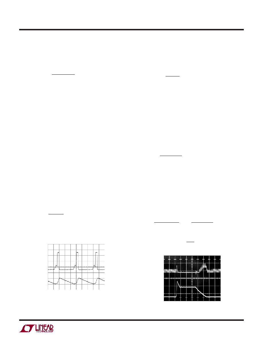
Figure 1. Lower Switching Frequency Occurs in High
Voltage Channel When Required On-Time Is Below 50ns
The maximum VIN should not exceed the absolute maxi-
mum rating. For fixed frequency operation, the maximum
VIN is:
V
DC
V
IN MAX
OUT
D
MIN
D
CE
(
) =
+
+
1
Note that the high voltage buck will still regulate at an input
voltage that exceeds VIN(MAX) (up to 35V). However, the
switching frequency will be lowered to satisfy the equa-
tion (Figure 1).
Oncetheinputvoltagereaches36.5V,aninternalovervoltage
lockout (OVLO) circuit is triggered to disable switching ac-
tion (Figure 2). Without switching, the LT3640 can sustain
VIN voltage transients up to 55V for one second.
VIN2 Voltage Range
The low voltage synchronous channel operates from
the VIN2 pin. The VIN2 pin can be connected to either an
independent voltage supply or the high voltage channel
output for a two-stage power regulator.
In either configuration, if the high voltage channel is over-
loadedandpulledoutofregulation,thelowvoltagechannel
will be disabled. The SS2 pin will be discharged as well.
The minimum VIN2 voltage to regulate output voltage is:
V
DC
IN MIN
OUT
MAX
2
(
) ≈
Where DCMAX is the maximum duty cycle (refer to
the Switching Frequency section). If VIN2 is below the
calculated minimum voltage, the output will fall out of
regulation.
The maximum VIN2 for fixed frequency operation is:
V
DC
IN MAX
OUT
MIN
2
(
) ≈
WhereDCMINistheminimumdutycycle (refertotheSwitch-
ing Frequency section). For voltage that exceeds VIN2(MAX)
(up to 5.5V), the low voltage channel exhi-bits pulse-skip-
ping behavior, and the output ripple will increase.
Inductor Selection
Inductorselectioninvolvesinductance,saturationcurrent,
series resistance (DCR) and magnetic loss.
The inductance for the high voltage channel is:
L
V
f
OUT
D
S
1 1 7
1
=
+
.
where VOUT1 is high voltage channel output voltage, VD
is the forward voltage drop of the catch diode, and fS is
the switching frequency. For example, 3.3H is a reason-
able inductance for a 3.3V output with 2MHz switching
frequency.
Oncetheinductanceisselected,theinductorcurrentripple
and peak current can be calculated:
I
V
I
f
V
L
OUT
D
L
S
OUT
D
IN
1
=
+
(
)
–
I
L PEAK
OUT MAX
L
(
)
(
)
=
+
2
Figure 2. VIN Overvoltage Lockout
applicaTions inForMaTion
200ns/DIV
SW1
10V/DIV
IL1
0.5A/DIV
3640 F01
VIN = 30V
VOUT1 = 3.3V/0.2A
RT SET = 2MHz
10s/DIV
VIN
20V/DIV
55VPK, 40V, 15V
IL1
2A/DIV
3640 F02
相关PDF资料 |
PDF描述 |
|---|---|
| LS4601-9RD2TB1 | 1-OUTPUT 100 W AC-DC PWR FACTOR CORR MODULE |
| LM3722E3.08MWC | 1-CHANNEL POWER SUPPLY SUPPORT CKT, UUC |
| L4973D5.1-013TR | 5.5 A SWITCHING REGULATOR, 300 kHz SWITCHING FREQ-MAX, PDSO20 |
| LSM-1.5/16-W3 | 1-OUTPUT DC-DC REG PWR SUPPLY MODULE |
| LM3354MM-4.1/NOPB | SWITCHED CAPACITOR REGULATOR, 1400 kHz SWITCHING FREQ-MAX, PDSO10 |
相关代理商/技术参数 |
参数描述 |
|---|---|
| LT3640EUFDTRPBF | 制造商:LINER 制造商全称:Linear Technology 功能描述:Dual Monolithic Buck Regulator with Power-On Reset and Watchdog Timer |
| LT3640IFE | 制造商:LINER 制造商全称:Linear Technology 功能描述:Dual Monolithic Buck Regulator with Power-On Reset and Watchdog Timer |
| LT3640IFE#PBF | 功能描述:IC REG BUCK FIX/ADJ DL 28TSSOP RoHS:是 类别:集成电路 (IC) >> PMIC - 稳压器 - DC DC 开关稳压器 系列:- 设计资源:Design Support Tool 标准包装:1 系列:- 类型:升压(升压) 输出类型:固定 输出数:1 输出电压:3V 输入电压:0.75 V ~ 2 V PWM 型:- 频率 - 开关:- 电流 - 输出:100mA 同步整流器:是 工作温度:-40°C ~ 85°C 安装类型:表面贴装 封装/外壳:SOT-23-5 细型,TSOT-23-5 包装:剪切带 (CT) 供应商设备封装:TSOT-23-5 其它名称:AS1323-BTTT-30CT |
| LT3640IFE#TRPBF | 功能描述:IC REG BUCK FIX/ADJ DL 28TSSOP RoHS:是 类别:集成电路 (IC) >> PMIC - 稳压器 - DC DC 开关稳压器 系列:- 设计资源:Design Support Tool 标准包装:1 系列:- 类型:升压(升压) 输出类型:固定 输出数:1 输出电压:3V 输入电压:0.75 V ~ 2 V PWM 型:- 频率 - 开关:- 电流 - 输出:100mA 同步整流器:是 工作温度:-40°C ~ 85°C 安装类型:表面贴装 封装/外壳:SOT-23-5 细型,TSOT-23-5 包装:剪切带 (CT) 供应商设备封装:TSOT-23-5 其它名称:AS1323-BTTT-30CT |
| LT3640IFEPBF | 制造商:LINER 制造商全称:Linear Technology 功能描述:Dual Monolithic Buck Regulator with Power-On Reset and Watchdog Timer |
发布紧急采购,3分钟左右您将得到回复。