- 您现在的位置:买卖IC网 > PDF目录14056 > LT3653EDCB#TRPBF (Linear Technology)IC REG BUCK ADJ 1.2A 8DFN PDF资料下载
参数资料
| 型号: | LT3653EDCB#TRPBF |
| 厂商: | Linear Technology |
| 文件页数: | 5/12页 |
| 文件大小: | 0K |
| 描述: | IC REG BUCK ADJ 1.2A 8DFN |
| 标准包装: | 2,500 |
| 类型: | 降压(降压) |
| 输出类型: | 可调式 |
| 输出数: | 1 |
| 输出电压: | 4.8 V ~ 6 V |
| 输入电压: | 7.5 V ~ 30 V |
| PWM 型: | 电流模式 |
| 频率 - 开关: | 1.5MHz |
| 电流 - 输出: | 1.2A |
| 同步整流器: | 无 |
| 工作温度: | -40°C ~ 125°C |
| 安装类型: | 表面贴装 |
| 封装/外壳: | 8-WFDFN 裸露焊盘 |
| 包装: | 带卷 (TR) |
| 供应商设备封装: | 8-DFN(3x2) |
�� �
�
�LT3653�
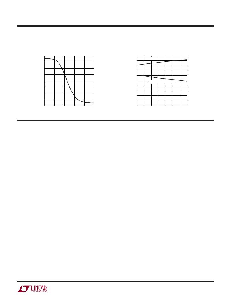
�TYPICAL� PERFORMANCE� CHARACTERISTICS�
�V� C� Current�
�T� A� =� 25°C� unless� otherwise� noted�
�V� C� Operating� Range�
�15�
�2.0�
�10�
�5�
�0�
�–5�
�–10�
�–15�
�–20�
�–25�
�1.8�
�1.6�
�1.4�
�1.2�
�1.0�
�0.8�
�0.6�
�0.4�
�0.2�
�0.0�
�CURRENT� LIMIT� CLAMP�
�SWITCHING� THRESHOLD�
�4�
�4.4�
�4.8� 5.2�
�5.6�
�6�
�-50�
�-25�
�0� 25� 50� 75�
�100�
�125�
�V� OUT� (V)�
�3653� G09�
�PIN� FUNCTIONS�
�V� IN� (Pin� 1):� The� V� IN� pin� supplies� current� to� the� LT3653’s�
�internal� regulator� and� the� internal� power� switch.� Locally�
�bypass� this� pin� with� a� capacitor.�
�HVOK� (Pin� 2):� The� HVOK� pin� is� a� status� pin� which� indi-�
�cates� that� the� internal� bias� rail� is� present� and� that� an� input�
�undervoltage� lockout� fault,� an� overvoltage� lockout� fault� or�
�an� over� temperature� fault� are� not� present.�
�V� C� (Pin� 3):� The� V� C� pin� is� the� output� of� the� internal� error�
�ampli?er� and� is� internally� compensated.� The� voltage� on� this�
�pin� controls� the� peak� switch� current.� Connect� this� pin� to�
�the� battery� charger� V� C� pin� for� battery� tracking� function.�
�I� LIM� (Pin� 4):� Connect� a� resistor� to� GND� to� program� the�
�output� current� limit� of� the� regulator.� See� the� I� LIM� Resistor�
�section� in� Application� Information.�
�V� OUT� (Pin� 5):� The� V� OUT� pin� is� connected� to� the� negative�
�TEMPERATURE� (oC)�
�3653� G10�
�I� SENSE� (Pin� 6):� The� I� SENSE� pin� is� the� positive� input� to� the�
�internal� current� sense� resistor� of� the� output� current� limit�
�circuit.� The� I� SENSE� pin� is� also� the� anode� of� the� internal�
�BOOST� diode.�
�BOOST� (Pin� 7):� The� BOOST� pin� provides� a� drive� voltage,�
�higher� than� the� input� voltage,� to� the� internal� power� switch.�
�The� BOOST� pin� is� internally� connected� to� the� cathode� of�
�the� BOOST� diode.�
�SW� (Pin� 8):� The� SW� pin� is� the� output� of� the� internal� power�
�switch.� Connect� this� pin� to� the� inductor,� catch� diode� and�
�boost� capacitor.�
�Exposed� Pad� (Pin� 9):� Ground.� The� Exposed� Pad� must� be�
�soldered� to� the� PCB� and� electrically� connected� to� ground.�
�Use� a� large� ground� plane� and� vias� to� optimize� thermal�
�performance.�
�terminal� of� the� internal� current� sense� resistor� of� the� output�
�current� limit� circuit.� Maximum� V� OUT� voltage� is� regulated�
�to� 4.8V.�
�3653f�
�5�
�相关PDF资料 |
PDF描述 |
|---|---|
| V24B6V5E200BF3 | CONVERTER MOD DC/DC 6.5V 200W |
| EEC60DREI-S13 | CONN EDGECARD 120POS .100 EXTEND |
| MAX6869UK38D3L+T | IC MPU SUPERVISOR SOT23-5 |
| V24B6V5E200BF2 | CONVERTER MOD DC/DC 6.5V 200W |
| LT3502AIMS#TRPBF | IC REG BUCK ADJ 0.5A 10MSOP |
相关代理商/技术参数 |
参数描述 |
|---|---|
| LT3653IDCB#TRMPBF | 功能描述:IC REG BUCK ADJ 1.2A 8DFN RoHS:是 类别:集成电路 (IC) >> PMIC - 稳压器 - DC DC 开关稳压器 系列:- 产品培训模块:Lead (SnPb) Finish for COTS Obsolescence Mitigation Program 标准包装:50 系列:- 类型:升压(升压) 输出类型:两者兼有 输出数:1 输出电压:5V,2 V ~ 16.5 V 输入电压:2 V ~ 16.5 V PWM 型:- 频率 - 开关:45kHz 电流 - 输出:50mA 同步整流器:无 工作温度:0°C ~ 70°C 安装类型:通孔 封装/外壳:8-DIP(0.300",7.62mm) 包装:管件 供应商设备封装:8-PDIP |
| LT3653IDCB#TRPBF | 功能描述:IC REG BUCK ADJ 1.2A 8DFN RoHS:是 类别:集成电路 (IC) >> PMIC - 稳压器 - DC DC 开关稳压器 系列:- 标准包装:2,500 系列:- 类型:降压(降压) 输出类型:固定 输出数:1 输出电压:1.2V,1.5V,1.8V,2.5V 输入电压:2.7 V ~ 20 V PWM 型:- 频率 - 开关:- 电流 - 输出:50mA 同步整流器:是 工作温度:-40°C ~ 125°C 安装类型:表面贴装 封装/外壳:10-TFSOP,10-MSOP(0.118",3.00mm 宽)裸露焊盘 包装:带卷 (TR) 供应商设备封装:10-MSOP 裸露焊盘 |
| LT3653IDCB-PBF | 制造商:LINER 制造商全称:Linear Technology 功能描述:1.2A, HV Input Regulator with Output Current Limit for Battery Charger Applications |
| LT3653IDCB-TRPBF | 制造商:LINER 制造商全称:Linear Technology 功能描述:1.2A, HV Input Regulator with Output Current Limit for Battery Charger Applications |
| LT3663EDCB#TRMPBF | 功能描述:IC REG BUCK ADJ 1.2A 8DFN RoHS:是 类别:集成电路 (IC) >> PMIC - 稳压器 - DC DC 开关稳压器 系列:- 标准包装:250 系列:- 类型:降压(降压) 输出类型:固定 输出数:1 输出电压:1.2V 输入电压:2.05 V ~ 6 V PWM 型:电压模式 频率 - 开关:2MHz 电流 - 输出:500mA 同步整流器:是 工作温度:-40°C ~ 85°C 安装类型:表面贴装 封装/外壳:6-UFDFN 包装:带卷 (TR) 供应商设备封装:6-SON(1.45x1) 产品目录页面:1032 (CN2011-ZH PDF) 其它名称:296-25628-2 |
发布紧急采购,3分钟左右您将得到回复。