- 您现在的位置:买卖IC网 > PDF目录14796 > LT3684IDD#PBF (Linear Technology)IC REG BUCK ADJ 2A 10DFN PDF资料下载
参数资料
| 型号: | LT3684IDD#PBF |
| 厂商: | Linear Technology |
| 文件页数: | 15/24页 |
| 文件大小: | 0K |
| 描述: | IC REG BUCK ADJ 2A 10DFN |
| 标准包装: | 121 |
| 类型: | 降压(降压) |
| 输出类型: | 可调式 |
| 输出数: | 1 |
| 输出电压: | 1.27 V ~ 20 V |
| 输入电压: | 3.6 V ~ 34 V |
| PWM 型: | 电流模式 |
| 频率 - 开关: | 300kHz ~ 3MHz |
| 电流 - 输出: | 2A |
| 同步整流器: | 无 |
| 工作温度: | -40°C ~ 125°C |
| 安装类型: | 表面贴装 |
| 封装/外壳: | 10-WFDFN 裸露焊盘 |
| 包装: | 管件 |
| 供应商设备封装: | 10-DFN(3x3) |
| 产品目录页面: | 1332 (CN2011-ZH PDF) |
�� �
�
�LT3684�
�APPLICATIONS� INFORMATION�
�BD�
�BOOST�
�V� OUT�
�6.0�
�5.5�
�TO� START�
�V� IN�
�V� IN�
�LT3684�
�C3�
�5.0�
�4.5�
�4.7� μ� F�
�GND�
�SW�
�4.0�
�TO� RUN�
�3.5�
�(4a)� For� V� OUT� >� 2.8V�
�3.0�
�2.5�
�2.0�
�V� OUT� =� 3.3V�
�T� A� =� 25� °� C�
�L� =� 4.7� μ� H�
�f� =� 800kHz�
�V� OUT�
�0.001�
�0.01�
�0.1�
�1�
�10�
�BD�
�BOOST�
�D2�
�8.0�
�LOAD� CURRENT� (A)�
�V� IN�
�V� IN�
�LT3684�
�C3�
�TO� START�
�7.0�
�4.7� μ� F�
�GND�
�SW�
�6.0�
�5.0�
�TO� RUN�
�(4b)� For� 2.5V� <� V� OUT� <� 2.8V�
�4.0�
�BD�
�V� OUT�
�3.0�
�2.0�
�V� OUT� =� 5V�
�T� A� =� 25� °� C�
�L� =� 4.7� μ� H�
�f� =� 800kHz�
�BOOST�
�0.001�
�0.01�
�0.1�
�1�
�10�
�V� IN�
�V� IN�
�LT3684�
�C3�
�LOAD� CURRENT� (A)�
�3684� F05�
�4.7� μ� F�
�GND�
�SW�
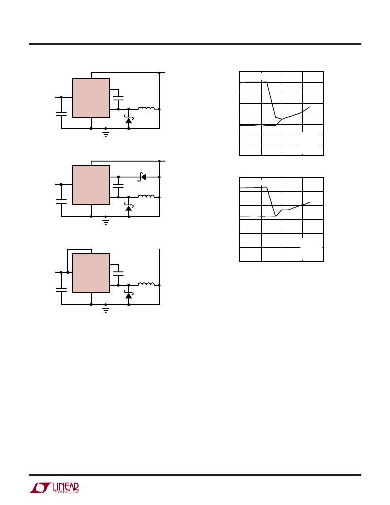
�Figure� 5.� The� Minimum� Input� Voltage� Depends� on�
�Output� Voltage,� Load� Current� and� Boost� Circuit�
�3684� FO4�
�voltage.� In� many� cases� the� discharged� output� capacitor�
�(4c)� For� V� OUT� <� 2.5V�
�Figure� 4.� Three� Circuits� For� Generating� The� Boost� Voltage�
�proper� start-up,� the� minimum� input� voltage� is� also� limited�
�by� the� boost� circuit.� If� the� input� voltage� is� ramped� slowly,�
�or� the� LT3684� is� turned� on� with� its� RUN/SS� pin� when� the�
�output� is� already� in� regulation,� then� the� boost� capacitor�
�may� not� be� fully� charged.� Because� the� boost� capacitor� is�
�charged� with� the� energy� stored� in� the� inductor,� the� circuit�
�will� rely� on� some� minimum� load� current� to� get� the� boost�
�circuit� running� properly.� This� minimum� load� will� depend�
�on� input� and� output� voltages,� and� on� the� arrangement� of�
�the� boost� circuit.� The� minimum� load� generally� goes� to�
�zero� once� the� circuit� has� started.� Figure� 5� shows� a� plot�
�of� minimum� load� to� start� and� to� run� as� a� function� of� input�
�will� present� a� load� to� the� switcher� and� the� minimum� input�
�to� start� will� be� the� same� as� the� minimum� input� to� run.�
�This� occurs,� for� example,� if� RUN/SS� is� asserted� after� V� IN�
�is� applied.� The� plots� show� the� worst-case� situation� where�
�V� IN� is� ramping� very� slowly.� For� lower� start-up� voltage,� the�
�boost� diode� can� be� tied� to� V� IN� ;� however,� this� restricts� the�
�input� range� to� one-half� of� the� absolute� maximum� rating�
�of� the� BOOST� pin.�
�At� light� loads,� the� inductor� current� becomes� discontinu-�
�ous� and� the� effective� duty� cycle� can� be� very� high.� This�
�reduces� the� minimum� input� voltage� to� approximately�
�300mV� above� V� OUT� .� At� higher� load� currents,� the� inductor�
�current� is� continuous� and� the� duty� cycle� is� limited� by� the�
�maximum� duty� cycle� of� the� LT3684,� requiring� a� higher�
�input� voltage� to� maintain� regulation.�
�3684f�
�15�
�相关PDF资料 |
PDF描述 |
|---|---|
| MAX6423XS40+T | IC MPU/RESET CIRC 4.00V SC70-4 |
| MAX6424UK38+T | IC MPU/RESET CIRC 3.80V SOT23-5 |
| 380LX821M160K022 | CAP ALUM 820UF 160V 20% SNAP |
| MAX6423XS35+T | IC MPU/RESET CIRC 3.50V SC70-4 |
| LLS2A182MELB | CAP ALUM 1800UF 100V 20% SNAP |
相关代理商/技术参数 |
参数描述 |
|---|---|
| LT3684IMSE | 制造商:LINER 制造商全称:Linear Technology 功能描述:36V, 2A, 2.8MHz Step-Down Switching Regulator |
| LT3684IMSE#PBF | 功能描述:IC REG BUCK ADJ 2A 10MSOP RoHS:是 类别:集成电路 (IC) >> PMIC - 稳压器 - DC DC 开关稳压器 系列:- 标准包装:250 系列:- 类型:降压(降压) 输出类型:固定 输出数:1 输出电压:1.2V 输入电压:2.05 V ~ 6 V PWM 型:电压模式 频率 - 开关:2MHz 电流 - 输出:500mA 同步整流器:是 工作温度:-40°C ~ 85°C 安装类型:表面贴装 封装/外壳:6-UFDFN 包装:带卷 (TR) 供应商设备封装:6-SON(1.45x1) 产品目录页面:1032 (CN2011-ZH PDF) 其它名称:296-25628-2 |
| LT3684IMSE#PBF | 制造商:Linear Technology 功能描述:DC-DC CONVERTER BUCK 2.8MHZ 制造商:Linear Technology 功能描述:DC-DC CONVERTER, BUCK, 2.8MHZ, MSOP-10 |
| LT3684IMSE#TRPBF | 功能描述:IC REG BUCK ADJ 2A 10MSOP RoHS:是 类别:集成电路 (IC) >> PMIC - 稳压器 - DC DC 开关稳压器 系列:- 设计资源:Design Support Tool 标准包装:1 系列:- 类型:升压(升压) 输出类型:固定 输出数:1 输出电压:3V 输入电压:0.75 V ~ 2 V PWM 型:- 频率 - 开关:- 电流 - 输出:100mA 同步整流器:是 工作温度:-40°C ~ 85°C 安装类型:表面贴装 封装/外壳:SOT-23-5 细型,TSOT-23-5 包装:剪切带 (CT) 供应商设备封装:TSOT-23-5 其它名称:AS1323-BTTT-30CT |
| LT3685 | 制造商:LINER 制造商全称:Linear Technology 功能描述:36V, 2.6A Monolithic Buck |
发布紧急采购,3分钟左右您将得到回复。