- 您现在的位置:买卖IC网 > PDF目录44986 > LT3686AIDD#TRPBF (LINEAR TECHNOLOGY CORP) 2.65 A SWITCHING REGULATOR, 2500 kHz SWITCHING FREQ-MAX, PDSO10 PDF资料下载
参数资料
| 型号: | LT3686AIDD#TRPBF |
| 厂商: | LINEAR TECHNOLOGY CORP |
| 元件分类: | 稳压器 |
| 英文描述: | 2.65 A SWITCHING REGULATOR, 2500 kHz SWITCHING FREQ-MAX, PDSO10 |
| 封装: | 3 X 3 MM, LEAD FREE, PLASTIC, MO-229WEED-2, DFN-10 |
| 文件页数: | 10/30页 |
| 文件大小: | 504K |
| 代理商: | LT3686AIDD#TRPBF |
第1页第2页第3页第4页第5页第6页第7页第8页第9页当前第10页第11页第12页第13页第14页第15页第16页第17页第18页第19页第20页第21页第22页第23页第24页第25页第26页第27页第28页第29页第30页
LT3686A
18
3686afa
ApplicAtions inForMAtion
below the minimum voltage to sustain boosted operation
(2.2V across the boost capacitor), the output voltage will
fall suddenly to:
VOUT = (VIN–2.2)DCMAX
Figure 9 shows the minimum VIN necessary to sustain
boosted operation during dropout. Once VIN drops below
the sustain voltage, VIN will need to reach the start voltage
again to refresh the boost capacitor. The programmable
undervoltagelockout(UVLO)functioncanbeusedtoavoid
operating unless VIN is greater than the start voltage.
Fixed Frequency at Light Load
The LT3686A contains unique active load circuitry to allow
for full frequency switching at very light loads. To enable
theactiveload,drivetheSYNC/MODEpinwithclockpulses
or a DC voltage greater than 0.8V.
Typical fixed frequency nonsynchronous buck regulators
skip pulses at light loads. With a fixed input voltage, as the
load current decreases in discontinuous mode, the regula-
tor is required to switch for shorter periods of time. When
therequiredontimedecreasesbelowthetypicalminimum
on time, the regulator skips one or more pulses so the
effective average duty cycle is equal to the required duty
cycle. This likelihood of entering pulse-skipping is exacer-
bated by the tendency for minimum on time to increase at
very light loads. Pulse-skipping is undesirable because it
causesunpredictable,sub-harmonicoutputripplethatcan
interfere with the operation of other sensitive components
such as AM receivers and audio equipment.
The BD active load is designed to combat pulse-skipping
by providing an operational regime between full frequency
discontinuous and pulse-skipping modes.
The maximum VIN before pulse-skipping in discontinu-
ous mode is directly dependent on load current; as the
load decreases, so does the pulse-skipping boundary. An
artificial load on the output helps push the pulse-skipping
boundary higher. The LT3686A achieves this goal by
commanding the minimum load necessary to keep itself
at full switching frequency, hence the circuitry is called
an active load.
As the LT3686A approaches minimum on time in dis-
continuous mode, its power switch transitions smoothly
into a fixed on time, fixed frequency, open loop current
source. Instead of controlling switch current, the internal
error amplifier servos the active load on the output via
the BD pin to maintain output voltage regulation. The
impact on efficiency is mitigated by pulling the minimum
current necessary to keep switching at full frequency. The
necessary BD load to maintain output regulation depends
on VIN, inductor size, and load current. As the necessary
BD load increases beyond its 40mA limit, pulse-skipping
mode will resume.
TheBDactiveloadcircuitryisenabledwhenMODEtiedhigh
and disabled when MODE is tied low. Even when activated,
the active load will shutdown when BD voltage exceeds
either 6V or VIN in an effort to minimize power dissipation
and intelligently react to external configurations.
To address the startup concerns delineated in the BOOST
and BD Pin Considerations section, the active load will
assist startup by pulling maximum current (40mA) to
charge the boost capacitor voltage in the absence of an
adequate load. An internal power good circuit will disable
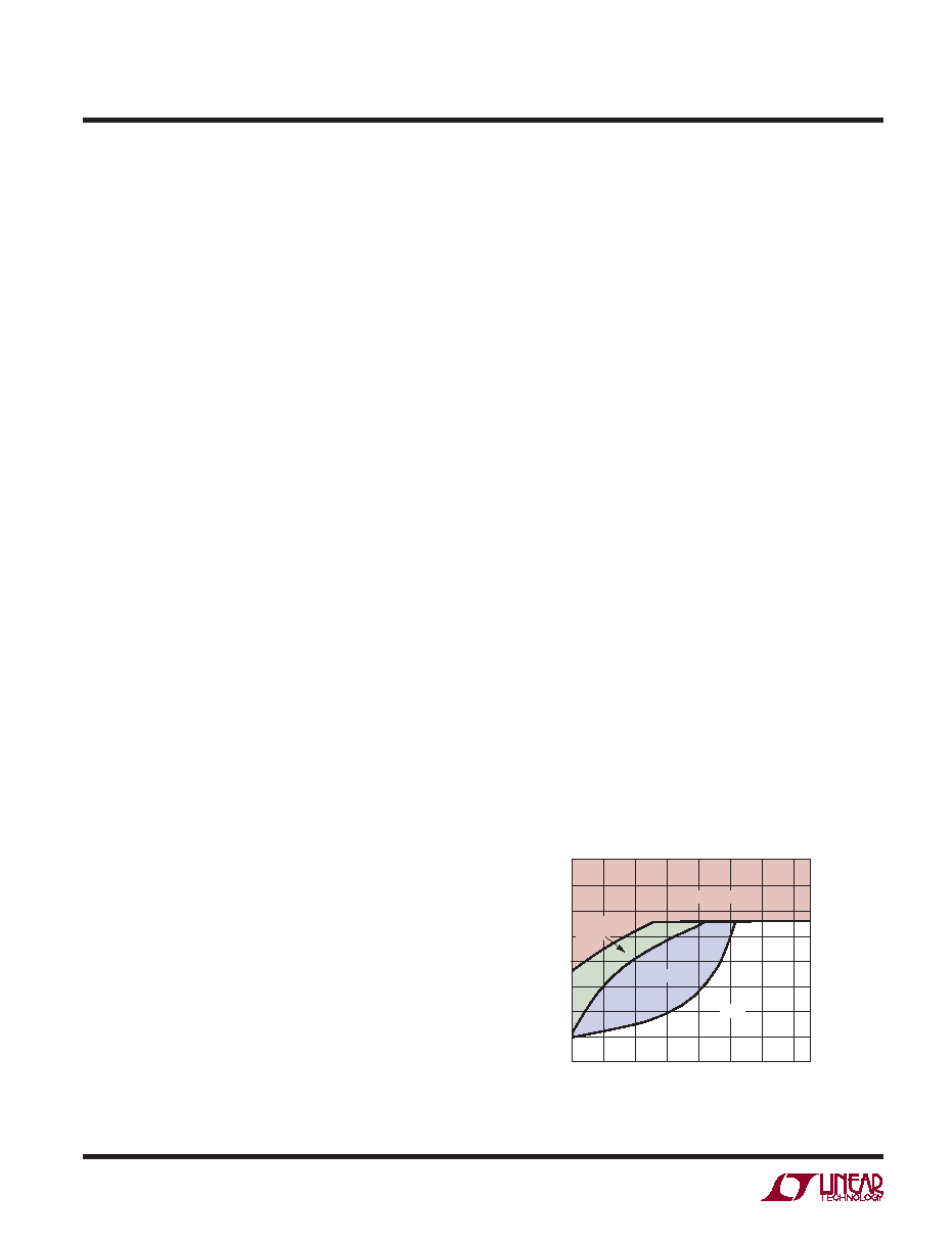
the BD active load when VFB reaches 0.7V. Figure 9 com-
pares plots of minimum input voltage to start and run as
a function of load current. In many cases the discharged
output capacitor will present a load to the switcher which
will allow it to start. The plots show the worst-case situ-
ation where VIN is ramping very slowly.
The active load also activates to hasten the recharge of
boost cap when operating beyond maximum duty cycle.
When not in use, the active load pulls no current.
Figure 10. Regions of Operation (5VOUT, 2MHz)
IOUT (mA)
0
V IN
(V)
5
10
20
25
35
30
40
15
20
40
60
100
120
140
80
3686A F10
CCM
DCM
ACTIVE
LOAD
PULSE-SKIPPING
相关PDF资料 |
PDF描述 |
|---|---|
| LT3686EDD#PBF | 2.65 A SWITCHING REGULATOR, 2500 kHz SWITCHING FREQ-MAX, PDSO10 |
| LT3686IDD#TRPBF | 2.65 A SWITCHING REGULATOR, 2500 kHz SWITCHING FREQ-MAX, PDSO10 |
| LT3688IFE#TRPBF | SWITCHING REGULATOR, PDSO24 |
| LT3688EUF#PBF | SWITCHING REGULATOR, PQCC24 |
| LT3688IFE#PBF | SWITCHING REGULATOR, PDSO24 |
相关代理商/技术参数 |
参数描述 |
|---|---|
| LT3686AIMSE#PBF | 功能描述:IC REG BUCK ADJ 1.2A 12MSOP RoHS:是 类别:集成电路 (IC) >> PMIC - 稳压器 - DC DC 开关稳压器 系列:- 标准包装:2,500 系列:- 类型:降压(降压) 输出类型:固定 输出数:1 输出电压:1.2V,1.5V,1.8V,2.5V 输入电压:2.7 V ~ 20 V PWM 型:- 频率 - 开关:- 电流 - 输出:50mA 同步整流器:是 工作温度:-40°C ~ 125°C 安装类型:表面贴装 封装/外壳:10-TFSOP,10-MSOP(0.118",3.00mm 宽)裸露焊盘 包装:带卷 (TR) 供应商设备封装:10-MSOP 裸露焊盘 |
| LT3686AIMSE#TRPBF | 功能描述:IC REG BUCK ADJ 1.2A 12MSOP RoHS:是 类别:集成电路 (IC) >> PMIC - 稳压器 - DC DC 开关稳压器 系列:- 标准包装:2,500 系列:- 类型:降压(降压) 输出类型:固定 输出数:1 输出电压:1.2V,1.5V,1.8V,2.5V 输入电压:2.7 V ~ 20 V PWM 型:- 频率 - 开关:- 电流 - 输出:50mA 同步整流器:是 工作温度:-40°C ~ 125°C 安装类型:表面贴装 封装/外壳:10-TFSOP,10-MSOP(0.118",3.00mm 宽)裸露焊盘 包装:带卷 (TR) 供应商设备封装:10-MSOP 裸露焊盘 |
| LT3686EDD | 制造商:LINER 制造商全称:Linear Technology 功能描述:37V/1.2A Step-Down Regulator in 3mm × 3mm DFN |
| LT3686EDD#PBF | 功能描述:IC REG BUCK ADJ 1.2A 10DFN RoHS:是 类别:集成电路 (IC) >> PMIC - 稳压器 - DC DC 开关稳压器 系列:- 标准包装:2,500 系列:- 类型:降压(降压) 输出类型:固定 输出数:1 输出电压:1.2V,1.5V,1.8V,2.5V 输入电压:2.7 V ~ 20 V PWM 型:- 频率 - 开关:- 电流 - 输出:50mA 同步整流器:是 工作温度:-40°C ~ 125°C 安装类型:表面贴装 封装/外壳:10-TFSOP,10-MSOP(0.118",3.00mm 宽)裸露焊盘 包装:带卷 (TR) 供应商设备封装:10-MSOP 裸露焊盘 |
| LT3686EDD#TRPBF | 功能描述:IC REG BUCK ADJ 1.2A 10DFN RoHS:是 类别:集成电路 (IC) >> PMIC - 稳压器 - DC DC 开关稳压器 系列:- 标准包装:2,500 系列:- 类型:降压(降压) 输出类型:固定 输出数:1 输出电压:1.2V,1.5V,1.8V,2.5V 输入电压:2.7 V ~ 20 V PWM 型:- 频率 - 开关:- 电流 - 输出:50mA 同步整流器:是 工作温度:-40°C ~ 125°C 安装类型:表面贴装 封装/外壳:10-TFSOP,10-MSOP(0.118",3.00mm 宽)裸露焊盘 包装:带卷 (TR) 供应商设备封装:10-MSOP 裸露焊盘 |
发布紧急采购,3分钟左右您将得到回复。