- 您现在的位置:买卖IC网 > PDF目录30768 > LT3695EMSE-3.3#PBF (LINEAR TECHNOLOGY CORP) 2 A SWITCHING REGULATOR, 2420 kHz SWITCHING FREQ-MAX, PDSO16 PDF资料下载
参数资料
| 型号: | LT3695EMSE-3.3#PBF |
| 厂商: | LINEAR TECHNOLOGY CORP |
| 元件分类: | 稳压器 |
| 英文描述: | 2 A SWITCHING REGULATOR, 2420 kHz SWITCHING FREQ-MAX, PDSO16 |
| 封装: | LEAD FREE, PLASTIC, MSOP-16 |
| 文件页数: | 11/30页 |
| 文件大小: | 491K |
| 代理商: | LT3695EMSE-3.3#PBF |
第1页第2页第3页第4页第5页第6页第7页第8页第9页第10页当前第11页第12页第13页第14页第15页第16页第17页第18页第19页第20页第21页第22页第23页第24页第25页第26页第27页第28页第29页第30页
LT3695 Series
19
3695fa
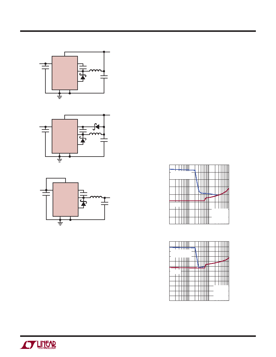
the output is already in regulation, then the boost capacitor
may not be fully charged. Because the boost capacitor is
charged with the energy stored in the inductor, the circuit
will rely on some minimum load current to get the boost
circuit running properly. This minimum load will depend
on input and output voltages, and on the arrangement of
the boost circuit. The minimum load generally goes to
zero once the circuit has started. Figure 5 shows a plot
of minimum load to start and to run as a function of input
voltage. In many cases the discharged output capacitor
will present a load to the switcher, which will allow it to
start. The plots show the worst-case situation where VIN is
ramping very slowly. For lower start-up voltage, the boost
diode can be tied to VIN; however, this restricts the input
range to one-half of the absolute maximum rating of the
BOOST pin. At light loads, the inductor current becomes
discontinuous and the effective duty cycle can be very high.
APPLICATIONS INFORMATION
BD
LT3695
VIN
C3
D1
VOUT
3695 F04a
BOOST
SW
DA
GND
PGND
(4a) For VOUT > 2.8V, VIN(MIN) = 4.3V if VOUT < 3V
BD
LT3695
VIN
C3
D1
D2
VOUT
3695 F04b
BOOST
SW
DA
GND
PGND
(4b) For 2.5V < VOUT < 2.8V, VIN(MIN) = 4.3V
BD
LT3695
VIN
C3
D1
VOUT
3695 F04c
BOOST
SW
DA
GND
PGND
(4c) For VOUT < 2.5V, VIN(MAX) = 25V
Figure 4. Three Circuits for Generating
the Boost Voltage for the LT3695
the circuit in Figure 4a. For higher output voltages, make
sure that there is no more than 8V at the BD pin either by
connecting it to another available supply higher than 3V or
by using a Zener diode between VOUT and BD to maintain
the BD pin voltage between 3V and 8V.
The minimum operating voltage of the LT3695 regulators
application is limited by the minimum input voltage and by
the maximum duty cycle as outlined previously. For proper
start-up, the minimum input voltage is also limited by the
boost circuit. If the input voltage is ramped slowly, or the
LT3695 regulators are turned on with their RUN/SS pin when
LOAD CURRENT (mA)
INPUT
VOL
TAGE
(V)
1
4.5
5.0
5.5
1000
3.5
4.0
3.0
2.5
2.0
10
100
10
100
6.0
LOAD CURRENT(mA)
INPUT
VOL
TAGE
(V)
3695 F05
1
6.0
6.5
7.0
7.5
1000
4.5
4.0
5.5
5.0
3.5
2.5
3.0
2.0
8.0
TO RUN
TO START
(WORST CASE)
TO START
(WORST CASE)
VOUT = 3.3V
TA = 25C
L = 10μH
f = 800kHz
TO RUN
VOUT = 5V
TA = 25C
L = 10μH
f = 800kHz
Figure 5. The Minimum Input Voltage Depends on
Output Voltage, Load Current and Boost Circuit
相关PDF资料 |
PDF描述 |
|---|---|
| LT3695EMSE-3.3#TRPBF | 2 A SWITCHING REGULATOR, 2420 kHz SWITCHING FREQ-MAX, PDSO16 |
| LT3751IUFD#TR | 1-CHANNEL POWER SUPPLY SUPPORT CKT, PQCC20 |
| LT3751IUFD#TRPBF | 1-CHANNEL POWER SUPPLY SUPPORT CKT, PQCC20 |
| LT3751EFE | 1-CHANNEL POWER SUPPLY SUPPORT CKT, PDSO20 |
| LT3751EUFD#TRPBF | 1-CHANNEL POWER SUPPLY SUPPORT CKT, PQCC20 |
相关代理商/技术参数 |
参数描述 |
|---|---|
| LT3695EMSE-5#PBF | 功能描述:IC REG BUCK 5V 1A 16MSOP RoHS:是 类别:集成电路 (IC) >> PMIC - 稳压器 - DC DC 开关稳压器 系列:- 标准包装:250 系列:- 类型:降压(降压) 输出类型:固定 输出数:1 输出电压:1.2V 输入电压:2.05 V ~ 6 V PWM 型:电压模式 频率 - 开关:2MHz 电流 - 输出:500mA 同步整流器:是 工作温度:-40°C ~ 85°C 安装类型:表面贴装 封装/外壳:6-UFDFN 包装:带卷 (TR) 供应商设备封装:6-SON(1.45x1) 产品目录页面:1032 (CN2011-ZH PDF) 其它名称:296-25628-2 |
| LT3695EMSE-5#PBF | 制造商:Linear Technology 功能描述:IC STEP-DOWN REGULATOR MSOP-16 |
| LT3695EMSE-5#TRPBF | 功能描述:IC REG BUCK 5V 1A 16MSOP RoHS:是 类别:集成电路 (IC) >> PMIC - 稳压器 - DC DC 开关稳压器 系列:- 标准包装:2,500 系列:- 类型:降压(降压) 输出类型:固定 输出数:1 输出电压:1.2V,1.5V,1.8V,2.5V 输入电压:2.7 V ~ 20 V PWM 型:- 频率 - 开关:- 电流 - 输出:50mA 同步整流器:是 工作温度:-40°C ~ 125°C 安装类型:表面贴装 封装/外壳:10-TFSOP,10-MSOP(0.118",3.00mm 宽)裸露焊盘 包装:带卷 (TR) 供应商设备封装:10-MSOP 裸露焊盘 |
| LT3695EMSEPBF | 制造商:LINER 制造商全称:Linear Technology 功能描述:1A Fault Tolerant Micropower Step-Down Regulator |
| LT3695EMSETRPBF | 制造商:LINER 制造商全称:Linear Technology 功能描述:1A Fault Tolerant Micropower Step-Down Regulator |
发布紧急采购,3分钟左右您将得到回复。