- 您现在的位置:买卖IC网 > PDF目录15308 > LT3759HMSE#TRPBF (Linear Technology)IC REG CTRLR BST INV PWM 12-MSOP PDF资料下载
参数资料
| 型号: | LT3759HMSE#TRPBF |
| 厂商: | Linear Technology |
| 文件页数: | 22/32页 |
| 文件大小: | 0K |
| 描述: | IC REG CTRLR BST INV PWM 12-MSOP |
| 标准包装: | 2,500 |
| PWM 型: | 电流模式 |
| 输出数: | 1 |
| 频率 - 最大: | 1MHz |
| 电源电压: | 1.6 V ~ 42 V |
| 降压: | 无 |
| 升压: | 是 |
| 回扫: | 无 |
| 反相: | 是 |
| 倍增器: | 无 |
| 除法器: | 无 |
| Cuk: | 无 |
| 隔离: | 无 |
| 工作温度: | -40°C ~ 150°C |
| 封装/外壳: | 12-TSSOP (0.118",3.00mm 宽)裸露焊盘 |
| 包装: | 带卷 (TR) |
第1页第2页第3页第4页第5页第6页第7页第8页第9页第10页第11页第12页第13页第14页第15页第16页第17页第18页第19页第20页第21页当前第22页第23页第24页第25页第26页第27页第28页第29页第30页第31页第32页
�� �
�
�LT3759�
�APPLICATIONS� INFORMATION�
�I� RMS(CDC)� ≥� I� O(MAX)� ?�
�I� D(PEAK)� =� ?� 1� +� ?� ?� I� O(MAX)� ?�
�V� OUT� –� V� D� D�
�For maximum efficiency, R� DS(ON)� and C� RSS� should be�
�minimized.� From� a� known� power� dissipated� in� the� power�
�MOSFET,� its� junction� temperature� can� be� obtained� using�
�the� following� equation:�
�T� J� =� T� A� +� P� FET� ?� θ� JA�
�=� T� A� +� P� FET� ?� (� θ� JC� +� θ� CA� )�
�T� J� must� not� exceed� the� MOSFET� maximum� junction�
�temperature� rating.� It� is� recommended� to� measure� the�
�MOSFET� temperature� in� steady� state� to� ensure� that� absolute�
�maximum� ratings� are� not� exceeded.�
�SEPIC� Converter:� Output� Diode� Selection�
�To� maximize� efficiency,� a� fast� switching� diode� with� a� low�
�forward� drop� and� low� reverse� leakage� is� desirable.� The�
�average� forward� current� in� normal� operation� is� equal� to�
�the� output� current,� and� the� peak� current� is� equal� to:�
�?� χ� ?� 1�
�?� 2� ?� 1� ?� D� MAX�
�It� is� recommended� that� the� peak� repetitive� reverse� voltage�
�rating� V� RRM� is� higher� than� V� OUT� +� V� IN(MAX)� by� a� safety�
�margin� (a� 10V� safety� margin� is� usually� sufficient).�
�The� power� dissipated� by� the� diode� is:�
�SEPIC� Converter:� Selecting� the� DC� Coupling� Capacitor�
�The� DC� voltage� rating� of� the� DC� coupling� capacitor� (C� DC� ,�
�as� shown� in� Figure� 1)� should� be� rated� for� the� maximum�
�input� voltage:�
�C� DC� ≥� V� IN(MAX)�
�C� DC� has� nearly� a� rectangular� current� waveform.� During�
�the� switch� off-time,� the� current� through� C� DC� is� I� IN� ,� while�
�approximately� –I� O� flows� during� the� on-time.� The� RMS�
�rating� of� the� coupling� capacitor� is� determined� by� the� fol-�
�lowing� equation:�
�V� OUT� +� V� D�
�V� IN(MIN)�
�A� low� ESR� and� ESL,� X5R� or� X7R� ceramic� capacitor� works�
�well� for� C� DC� .�
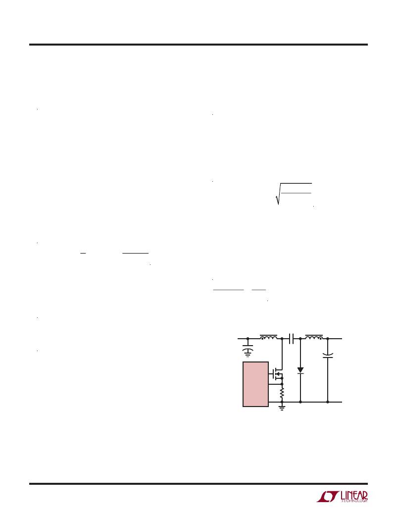
�INVERTING� CONVERTER� APPLICATIONS�
�The� LT3759� can� be� configured� as� a� dual-inductor� inverting�
�topology,� as� shown� in� Figure� 9.� The� V� OUT� to� V� IN� ratio� is:�
�=�
�V� IN� 1� ?� D�
�In� continuous� conduction� mode� (CCM).�
�P� D� =� I� O(MAX)� ?� V� D�
�and� the� diode� junction� temperature� is:�
�T� J� =� T� A� +� P� D� ?� R� θ� JA�
�The� R� θ� JA� used� in� this� equation� normally� includes� the� R� θ� JC�
�for� the� device,� plus� the� thermal� resistance� from� the� board,�
�to� the� ambient� temperature� in� the� enclosure.� T� J� must� not�
�exceed� the� diode� maximum� junction� temperature� rating.�
�V� IN�
�+�
�L1�
�C� IN�
�LT3759�
�GATE�
�SENSE�
�GND�
�C� DC�
�+� –�
�M1�
�R� SENSE�
�D1�
�L2�
�+�
�–�
�C� OUT�
�V� OUT�
�+�
�3759� F09�
�SEPIC� Converter:� Output� and� Input� Capacitor� Selection�
�The� selections� of� the� output� and� input� capacitors� of� the�
�SEPIC� converter� are� similar� to� those� of� the� boost� converter.�
�Please� refer� to� the� Boost� Converter,� Output� Capacitor�
�Selection� and� Boost� Converter,� Input� Capacitor� Selection�
�sections.�
�Figure� 9.� A� Simplified� Inverting� Converter�
�3759fc�
�22�
�For� more� information� www.linear.com/3759�
�相关PDF资料 |
PDF描述 |
|---|---|
| GBC55DCST-S288 | CONN EDGECARD 110POS .100 EXTEND |
| LTC3869IUFD#TRPBF | IC REG CTRLR BUCK PWM CM 28-QFN |
| TVX1E471MCD | CAP ALUM 470UF 25V 20% AXIAL |
| LTC3869IGN-2#TRPBF | IC REG CTRLR BUCK PWM CM 28-SSOP |
| LTC3869IGN-2#PBF | IC REG CTRLR BUCK PWM CM 28-SSOP |
相关代理商/技术参数 |
参数描述 |
|---|---|
| LT3759IMSE#PBF | 功能描述:IC REG CTRLR BST INV PWM 12-MSOP RoHS:是 类别:集成电路 (IC) >> PMIC - 稳压器 - DC DC 切换控制器 系列:- 标准包装:2,500 系列:- PWM 型:电流模式 输出数:1 频率 - 最大:500kHz 占空比:96% 电源电压:4 V ~ 36 V 降压:无 升压:是 回扫:无 反相:无 倍增器:无 除法器:无 Cuk:无 隔离:无 工作温度:-40°C ~ 125°C 封装/外壳:24-WQFN 裸露焊盘 包装:带卷 (TR) |
| LT3759IMSE#TRPBF | 功能描述:IC REG CTRLR BST INV PWM 12-MSOP RoHS:是 类别:集成电路 (IC) >> PMIC - 稳压器 - DC DC 切换控制器 系列:- 标准包装:2,500 系列:- PWM 型:电流模式 输出数:1 频率 - 最大:500kHz 占空比:96% 电源电压:4 V ~ 36 V 降压:无 升压:是 回扫:无 反相:无 倍增器:无 除法器:无 Cuk:无 隔离:无 工作温度:-40°C ~ 125°C 封装/外壳:24-WQFN 裸露焊盘 包装:带卷 (TR) |
| LT375B | 制造商:EDSYN 功能描述:TIP SPADE 1.5X12.2MM |
| LT375-C | 制造商:EDSYN 功能描述: |
| LT376 | 制造商:EDSYN 功能描述: 制造商:EDSYN 功能描述:SOLDERING TIP, Tip / Nozzle Length:0.48" |
发布紧急采购,3分钟左右您将得到回复。