- 您现在的位置:买卖IC网 > PDF目录14831 > LT3970EMS#PBF (Linear Technology)IC REG BUCK ADJ 0.35A 10MSOP PDF资料下载
参数资料
| 型号: | LT3970EMS#PBF |
| 厂商: | Linear Technology |
| 文件页数: | 16/22页 |
| 文件大小: | 0K |
| 描述: | IC REG BUCK ADJ 0.35A 10MSOP |
| 标准包装: | 50 |
| 类型: | 降压(降压) |
| 输出类型: | 可调式 |
| 输出数: | 1 |
| 输出电压: | 1.21 V ~ 25 V |
| 输入电压: | 4.2 V ~ 40 V |
| PWM 型: | 电流模式,Burst Mode? |
| 频率 - 开关: | 200kHz ~ 2.25MHz |
| 电流 - 输出: | 350mA |
| 同步整流器: | 无 |
| 工作温度: | -40°C ~ 125°C |
| 安装类型: | 表面贴装 |
| 封装/外壳: | 10-TFSOP,10-MSOP(0.118",3.00mm 宽) |
| 包装: | 管件 |
| 供应商设备封装: | 10-MSOP |
| 产品目录页面: | 1332 (CN2011-ZH PDF) |
�� �
�
�LT3970� Series�
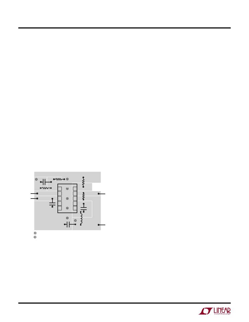
�APPLICATIONS� INFORMATION�
�PCB� Layout�
�For� proper� operation� and� minimum� EMI,� care� must� be�
�taken� during� printed� circuit� board� layout.� Figure� 9� shows�
�the� recommended� component� placement� with� trace,�
�ground� plane� and� via� locations.� Note� that� large,� switched�
�currents� flow� in� the� LT3970’s� V� IN� and� SW� pins,� the� internal�
�catch� diode� and� the� input� capacitor.� The� loop� formed� by�
�these� components� should� be� as� small� as� possible.� These�
�components,� along� with� the� inductor� and� output� capacitor,�
�should� be� placed� on� the� same� side� of� the� circuit� board,�
�and� their� connections� should� be� made� on� that� layer.� Place�
�a� local,� unbroken� ground� plane� below� these� components.�
�The� SW� and� BOOST� nodes� should� be� as� small� as� possible.�
�Finally,� keep� the� FB� nodes� small� so� that� the� ground� traces�
�will� shield� them� from� the� SW� and� BOOST� nodes.� The�
�Exposed� Pad� on� the� bottom� of� the� DFN� package� must� be�
�soldered� to� ground� so� that� the� pad� acts� as� a� heat� sink.� To�
�keep� thermal� resistance� low,� extend� the� ground� plane� as�
�much� as� possible,� and� add� thermal� vias� under� and� near�
�the� LT3970� to� additional� ground� planes� within� the� circuit�
�board� and� on� the� bottom� side.�
�GND�
�with� stray� inductance� in� series� with� the� power� source,�
�forms� an� under� damped� tank� circuit,� and� the� voltage� at�
�the� V� IN� pin� of� the� LT3970� can� ring� to� twice� the� nominal�
�input� voltage,� possibly� exceeding� the� LT3970’s� rating� and�
�damaging� the� part.� If� the� input� supply� is� poorly� controlled�
�or� the� user� will� be� plugging� the� LT3970� into� an� energized�
�supply,� the� input� network� should� be� designed� to� prevent�
�this� overshoot.� See� Linear� Technology� Application� Note� 88�
�for� a� complete� discussion.�
�High� Temperature� Considerations�
�For� higher� ambient� temperatures,� care� should� be� taken�
�in� the� layout� of� the� PCB� to� ensure� good� heat� sinking�
�of� the� LT3970.� The� Exposed� Pad� on� the� bottom� of� the�
�DFN� package� must� be� soldered� to� a� ground� plane.� This�
�ground� should� be� tied� to� large� copper� layers� below� with�
�thermal� vias;� these� layers� will� spread� the� heat� dissipated�
�by� the� LT3970.� Placing� additional� vias� can� reduce� thermal�
�resistance� further.� In� the� MSOP� package,� the� copper� lead�
�frame� is� fused� to� GND� (Pin� 5)� so� place� thermal� vias� near�
�this� pin.� The� maximum� load� current� should� be� derated�
�as� the� ambient� temperature� approaches� the� maximum�
�junction� rating.�
�EN�
�V� IN�
�1� 10�
�2� 9�
�3� 8�
�4� 7�
�5� 6�
�GND�
�VIAS� TO� LOCAL� GROUND� PLANE�
�GND�
�3970� F09�
�PG�
�V� OUT�
�Power� dissipation� within� the� LT3970� can� be� estimated� by�
�calculating� the� total� power� loss� from� an� efficiency� measure-�
�ment� and� subtracting� inductor� loss.� The� die� temperature�
�is� calculated� by� multiplying� the� LT3970� power� dissipation�
�by� the� thermal� resistance� from� junction� to� ambient.�
�Finally,� be� aware� that� at� high� ambient� temperatures� the�
�internal� Schottky� diode� will� have� significant� leakage� current�
�(see� Typical� Performance� Characteristics)� increasing� the�
�quiescent� current� of� the� LT3970� converter.�
�VIAS� TO� V� OUT�
�Figure� 9.� A� Good� PCB� Layout� Ensures� Proper,� Low� EMI� Operation�
�Hot� Plugging� Safely�
�The� small� size,� robustness� and� low� impedance� of� ceramic�
�capacitors� make� them� an� attractive� option� for� the� input�
�bypass� capacitor� of� LT3970� circuits.� However,� these� ca-�
�pacitors� can� cause� problems� if� the� LT3970� is� plugged� into�
�a� live� supply.� The� low� loss� ceramic� capacitor,� combined�
�16�
�Other� Linear� Technology� Publications�
�Application� Notes� 19,� 35� and� 44� contain� more� detailed�
�descriptions� and� design� information� for� buck� regulators�
�and� other� switching� regulators.� The� LT1376� data� sheet�
�has� a� more� extensive� discussion� of� output� ripple,� loop�
�compensation� and� stability� testing.� Design� Note� 100�
�shows� how� to� generate� a� bipolar� output� supply� using� a�
�buck� regulator.�
�3970fc�
�相关PDF资料 |
PDF描述 |
|---|---|
| RBM36DCTN-S288 | CONN EDGECARD 72POS .156 EXTEND |
| GBM36DTBD | CONN EDGECARD 72POS R/A .156 SLD |
| RBM36DCTH-S288 | CONN EDGECARD 72POS .156 EXTEND |
| GBM36DTAN | CONN EDGECARD 72POS R/A .156 SLD |
| LT3580IMS8E#PBF | IC REG BOOST INV SEPIC 2A 8MSOP |
相关代理商/技术参数 |
参数描述 |
|---|---|
| LT3970EMS-TRPBF | 制造商:LINER 制造商全称:Linear Technology 功能描述:40V, 350mA Step-Down Regulator with 2.5μA Quiescent Current and Integrated Diodes |
| LT3970HMS#PBF | 制造商:Linear Technology 功能描述:IC REG BUCK ADJ 0.35A 10MSOP 制造商:Linear Technology 功能描述:IC, STEP DOWN REG, 200KHZ-2.2MHZ, MSOP10 制造商:Linear Technology 功能描述:SWITCHING REG, BUCK, ADJ, 2.2MHZ, MSOP10, Primary Input Voltage:40V, No. of Outputs:1, Output Current:350mA, No. of Pins:10, Operating Temperature Min:-40C, Operating Temperature Max:150C, Package / Case:10-MSOP , RoHS Compliant: Yes |
| LT3970HMS#TRPBF | 制造商:Linear Technology 功能描述:IC REG BUCK ADJ 0.35A 10MSOP 制造商:Linear Technology 功能描述:SWITCHING REG, BUCK, ADJ, 2.2MHZ, MSOP10, Primary Input Voltage:40V, No. of Outputs:1, Output Current:350mA, No. of Pins:10, Operating Temperature Min:-40C, Operating Temperature Max:150C, Package / Case:10-MSOP , RoHS Compliant: Yes |
| LT3970HMS-3.3#PBF | 功能描述:IC REG BUCK 3.3V 0.35A 10MSOP RoHS:是 类别:集成电路 (IC) >> PMIC - 稳压器 - DC DC 开关稳压器 系列:- 标准包装:2,500 系列:- 类型:降压(降压) 输出类型:固定 输出数:1 输出电压:1.2V,1.5V,1.8V,2.5V 输入电压:2.7 V ~ 20 V PWM 型:- 频率 - 开关:- 电流 - 输出:50mA 同步整流器:是 工作温度:-40°C ~ 125°C 安装类型:表面贴装 封装/外壳:10-TFSOP,10-MSOP(0.118",3.00mm 宽)裸露焊盘 包装:带卷 (TR) 供应商设备封装:10-MSOP 裸露焊盘 |
| LT3970HMS-3.3#TRPBF | 功能描述:IC REG BUCK 3.3V 0.35A 10MSOP RoHS:是 类别:集成电路 (IC) >> PMIC - 稳压器 - DC DC 开关稳压器 系列:- 标准包装:2,500 系列:- 类型:降压(降压) 输出类型:固定 输出数:1 输出电压:1.2V,1.5V,1.8V,2.5V 输入电压:2.7 V ~ 20 V PWM 型:- 频率 - 开关:- 电流 - 输出:50mA 同步整流器:是 工作温度:-40°C ~ 125°C 安装类型:表面贴装 封装/外壳:10-TFSOP,10-MSOP(0.118",3.00mm 宽)裸露焊盘 包装:带卷 (TR) 供应商设备封装:10-MSOP 裸露焊盘 |
发布紧急采购,3分钟左右您将得到回复。