- 您现在的位置:买卖IC网 > PDF目录6081 > LT6200CS6#TRMPBF (Linear Technology)IC OPAMP R-R I/O 165MHZ SOT-23-6 PDF资料下载
参数资料
| 型号: | LT6200CS6#TRMPBF |
| 厂商: | Linear Technology |
| 文件页数: | 13/26页 |
| 文件大小: | 0K |
| 描述: | IC OPAMP R-R I/O 165MHZ SOT-23-6 |
| 标准包装: | 1 |
| 放大器类型: | 缓冲器 |
| 电路数: | 1 |
| 输出类型: | 满摆幅 |
| 转换速率: | 50 V/µs |
| 增益带宽积: | 165MHz |
| 电流 - 输入偏压: | 23µA |
| 电压 - 输入偏移: | 2500µV |
| 电流 - 电源: | 20mA |
| 电流 - 输出 / 通道: | 90mA |
| 电压 - 电源,单路/双路(±): | 2.5 V ~ 12.6 V,±1.25 V ~ 6.3 V |
| 工作温度: | 0°C ~ 70°C |
| 安装类型: | 表面贴装 |
| 封装/外壳: | SOT-23-6 |
| 供应商设备封装: | TSOT-23-6 |
| 包装: | 标准包装 |
| 产品目录页面: | 1320 (CN2011-ZH PDF) |
| 其它名称: | LT6200CS6#TRMPBFDKR |
LT6200/LT6200-5
LT6200-10/LT6201
20
62001ff
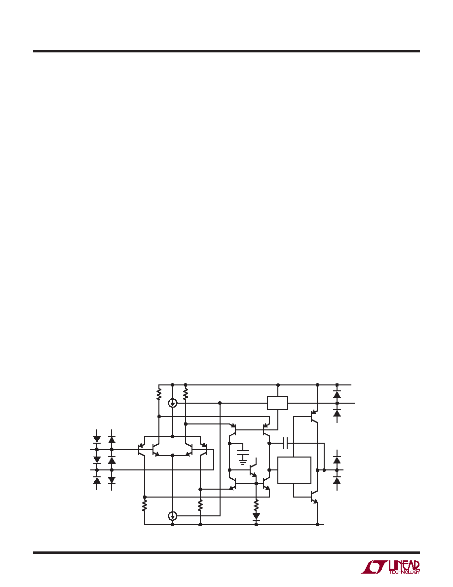
applicaTions inForMaTion
Amplifier Characteristics
Figure 1 shows a simplified schematic of the LT6200
family, which has two input differential amplifiers in paral-
lel that are biased on simultaneously when the common
mode voltage is at least 1.5V from either rail. This topology
allows the input stage to swing from the positive supply
voltage to the negative supply voltage. As the common
mode voltage swings beyond VCC– 1.5V, current source I1
saturates and current in Q1/Q4 is zero. Feedback is main-
tained through the Q2/Q3 differential amplifier, but with
an input gm reduction of one-half. A similar effect occurs
with I2 when the common mode voltage swings within
1.5V of the negative rail. The effect of the gm reduction is
a shift in the VOS as I1 or I2 saturate.
Input bias current normally flows out of the “+” and “–”
inputs. The magnitude of this current increases when the
input common mode voltage is within 1.5V of the negative
rail, and only Q1/Q4 are active. The polarity of this current
reverses when the input common mode voltage is within
1.5V of the positive rail and only Q2/Q3 are active.
The second stage is a folded cascode and current mir-
ror that converts the input stage differential signals to a
single ended output. Capacitor C1 reduces the unity cross
frequency and improves the frequency stability with-
out degrading the gain bandwidth of the amplifier. The
differential drive generator supplies current to the output
transistors that swing from rail-to-rail.
The LT6200-5/LT6200-10 are decompensated op amps
for higher gain applications. These amplifiers maintain
identical DC specifications with the LT6200, but have a
reduced Miller compensation capacitor CM. This results
in a significantly higher slew rate and gain bandwidth
product.
Input Protection
There are back-to-back diodes, D1 and D2, across the
+ and – inputs of these amplifiers to limit the differential
input voltage to ±0.7V. The inputs of the LT6200 family
do not have internal resistors in series with the input
transistors. This technique is often used to protect the
input devices from overvoltage that causes excessive
currents to flow. The addition of these resistors would
significantly degrade the low noise voltage of these
amplifiers. For instance, a 100Ω resistor in series with
each input would generate 1.8nV/√Hz of noise, and the
total amplifier noise voltage would rise from 0.95nV/√Hz
to 2.03nV/√Hz. Once the input differential voltage ex-
ceeds ±0.7V, steady-state current conducted though
the protection diodes should be limited to ±40mA.
This implies 25Ω of protection resistance per volt of
continuous overdrive beyond ±0.7V. The input diodes
are rugged enough to handle transient currents due to
amplifier slew rate overdrive or momentary clipping
without these resistors.
DIFFERENTIAL
DRIVE
GENERATOR
R1
R2
R3
R4
R5
Q2
Q3
Q5
Q6
Q9
Q8
Q7
Q10
Q11
Q1
Q4
I1
I2
D3
D2
D1
DESD2
DESD4
DESD3
DESD1
DESD5
DESD8
DESD7
DESD6
+
–
CM
C1
+V
–V
+V
–V
V+
V–
6203/04 F01
BIAS
VSHDN
Figure 1. Simplified Schematic
相关PDF资料 |
PDF描述 |
|---|---|
| 929834-02-08 | CONN HEADER .100 SNGL STR 8POS |
| 960244-8100-AR-TP | CONN SOCKET 44POS 2ROW BRDMT SMD |
| 61201622021 | HEADER 16POS PIN LATCH PCB 2ROW |
| 953464-6602-AR | CONN SOCKET 64POS 2MM VERT DUAL |
| 61201622821 | HEADER 16POS PIN LATCH PCB 2ROW |
相关代理商/技术参数 |
参数描述 |
|---|---|
| LT6200CS6TRPBF | 制造商:LINER 制造商全称:Linear Technology 功能描述:165MHz, Rail-to-Rail Input and Output, 0.95nV/√Hz Low Noise, Op Amp Family |
| LT6200CS8 | 功能描述:IC OPAMP R-R I/O 165MHZ 8-SOIC RoHS:否 类别:集成电路 (IC) >> Linear - Amplifiers - Instrumentation 系列:- 标准包装:50 系列:LinCMOS™ 放大器类型:通用 电路数:4 输出类型:- 转换速率:0.05 V/µs 增益带宽积:110kHz -3db带宽:- 电流 - 输入偏压:0.7pA 电压 - 输入偏移:210µV 电流 - 电源:57µA 电流 - 输出 / 通道:30mA 电压 - 电源,单路/双路(±):3 V ~ 16 V,±1.5 V ~ 8 V 工作温度:-40°C ~ 85°C 安装类型:表面贴装 封装/外壳:14-SOIC(0.154",3.90mm 宽) 供应商设备封装:14-SOIC 包装:管件 产品目录页面:865 (CN2011-ZH PDF) 其它名称:296-1834296-1834-5 |
| LT6200CS8#PBF | 功能描述:IC OPAMP R-R I/O 165MHZ 8-SOIC RoHS:是 类别:集成电路 (IC) >> Linear - Amplifiers - Instrumentation 系列:- 产品培训模块:Differential Circuit Design Techniques for Communication Applications 标准包装:1 系列:- 放大器类型:RF/IF 差分 电路数:1 输出类型:差分 转换速率:9800 V/µs 增益带宽积:- -3db带宽:2.9GHz 电流 - 输入偏压:3µA 电压 - 输入偏移:- 电流 - 电源:40mA 电流 - 输出 / 通道:- 电压 - 电源,单路/双路(±):3 V ~ 3.6 V 工作温度:-40°C ~ 85°C 安装类型:表面贴装 封装/外壳:16-VQFN 裸露焊盘,CSP 供应商设备封装:16-LFCSP-VQ 包装:剪切带 (CT) 产品目录页面:551 (CN2011-ZH PDF) 其它名称:ADL5561ACPZ-R7CT |
| LT6200CS8#TR | 功能描述:IC OPAMP R-R I/O 165MHZ 8SOIC RoHS:否 类别:集成电路 (IC) >> Linear - Amplifiers - Instrumentation 系列:- 标准包装:50 系列:LinCMOS™ 放大器类型:通用 电路数:4 输出类型:- 转换速率:0.05 V/µs 增益带宽积:110kHz -3db带宽:- 电流 - 输入偏压:0.7pA 电压 - 输入偏移:210µV 电流 - 电源:57µA 电流 - 输出 / 通道:30mA 电压 - 电源,单路/双路(±):3 V ~ 16 V,±1.5 V ~ 8 V 工作温度:-40°C ~ 85°C 安装类型:表面贴装 封装/外壳:14-SOIC(0.154",3.90mm 宽) 供应商设备封装:14-SOIC 包装:管件 产品目录页面:865 (CN2011-ZH PDF) 其它名称:296-1834296-1834-5 |
| LT6200CS8#TRPBF | 功能描述:IC OPAMP R-R I/O 165MHZ 8-SOIC RoHS:是 类别:集成电路 (IC) >> Linear - Amplifiers - Instrumentation 系列:- 标准包装:50 系列:LinCMOS™ 放大器类型:通用 电路数:4 输出类型:- 转换速率:0.05 V/µs 增益带宽积:110kHz -3db带宽:- 电流 - 输入偏压:0.7pA 电压 - 输入偏移:210µV 电流 - 电源:57µA 电流 - 输出 / 通道:30mA 电压 - 电源,单路/双路(±):3 V ~ 16 V,±1.5 V ~ 8 V 工作温度:-40°C ~ 85°C 安装类型:表面贴装 封装/外壳:14-SOIC(0.154",3.90mm 宽) 供应商设备封装:14-SOIC 包装:管件 产品目录页面:865 (CN2011-ZH PDF) 其它名称:296-1834296-1834-5 |
发布紧急采购,3分钟左右您将得到回复。