- 您现在的位置:买卖IC网 > PDF目录2155 > LT6211CDD#TRPBF (Linear Technology)IC AMP CURR FDBK DUAL R-R 10DFN PDF资料下载
参数资料
| 型号: | LT6211CDD#TRPBF |
| 厂商: | Linear Technology |
| 文件页数: | 4/18页 |
| 文件大小: | 0K |
| 描述: | IC AMP CURR FDBK DUAL R-R 10DFN |
| 标准包装: | 2,500 |
| 放大器类型: | 电流反馈 |
| 电路数: | 2 |
| 输出类型: | 满摆幅 |
| 转换速率: | 700 V/µs |
| -3db带宽: | 200MHz |
| 电流 - 输入偏压: | 13.5µA |
| 电压 - 输入偏移: | 1000µV |
| 电流 - 电源: | 6mA |
| 电流 - 输出 / 通道: | 75mA |
| 电压 - 电源,单路/双路(±): | 3 V ~ 12 V,±1.5 V ~ 6 V |
| 工作温度: | 0°C ~ 70°C |
| 安装类型: | 表面贴装 |
| 封装/外壳: | 10-WFDFN 裸露焊盘 |
| 供应商设备封装: | 10-DFN-EP(3x3) |
| 包装: | 带卷 (TR) |
LT6210/LT6211
12
62101fc
applicaTions inForMaTion
Setting the Quiescent Operating Current (ISET Pin)
The quiescent bias point of the LT6210/LT6211 is SET
with either an external resistor from the ISET pin to a
lower potential or by drawing a current out of the ISET
pin. However, the ISET pin is not designed to function as a
shutdown. The LT6211 uses two entirely independent bias
networks, so while each channel can be programmed for
a different supply current, neither ISET pin should be left
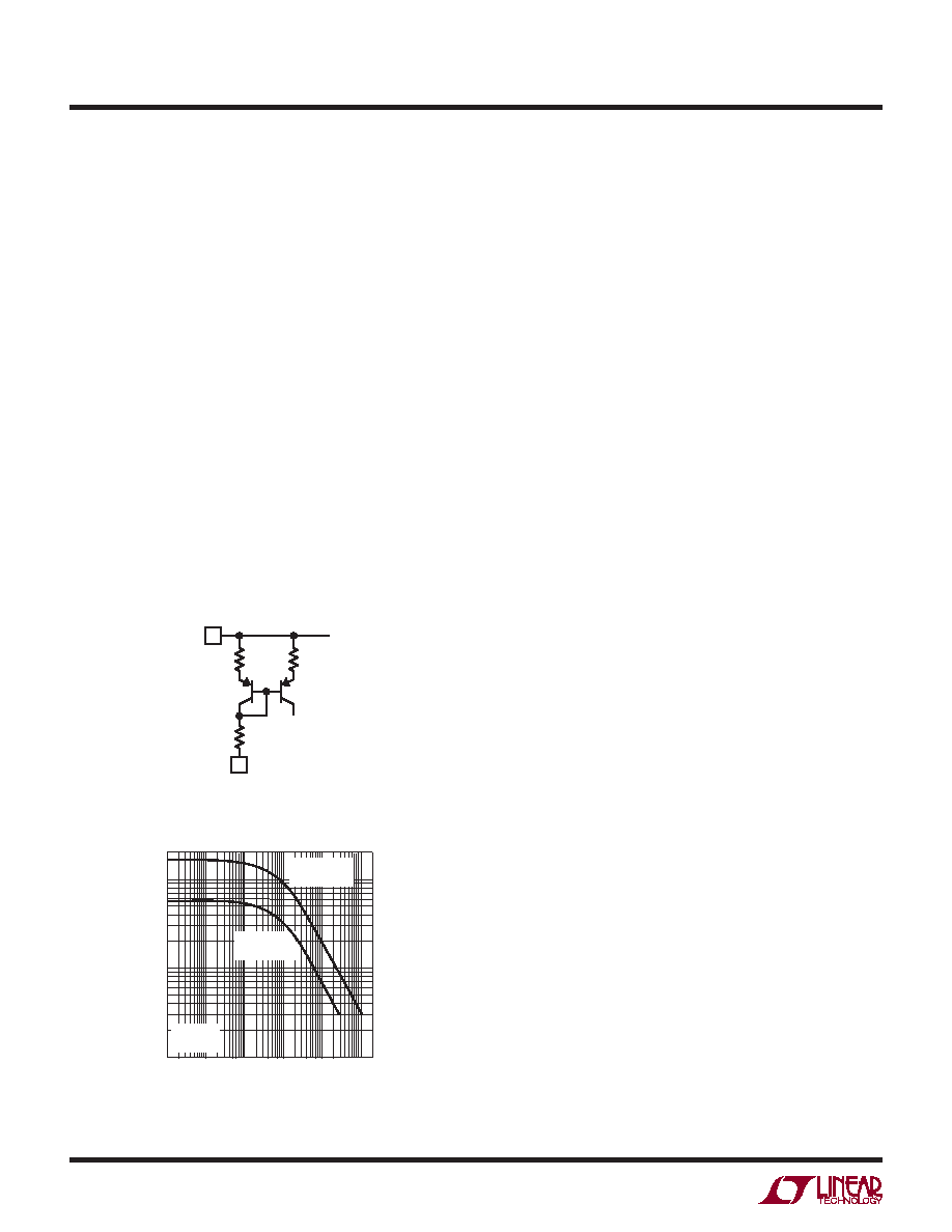
unconnected. A simplified schematic of the internal bias-
ing structure can be seen in Figure 1. Figure 2 illustrates
the results of varying RSET on 3V and ±5V supplies. Note
that shorting the ISET pin under 3V operation results in
a quiescent bias of approximately 6mA. Attempting to
bias the LT6210/LT6211 at a current level higher than
6mA by using a smaller resistor may result in instability
and decreased performance. However, internal circuitry
clamps the supply current of the part at a safe level of
approximately 15mA in case of accidental connection of
the ISET pin directly to a negative potential.
Input Considerations
The inputs of the LT6210/LT6211 are protected by back-
to-back diodes. If the differential input voltage exceeds
1.4V, the input current should be limited to less than the
absolute maximum ratings of ±10mA. In normal opera-
tion, the differential voltage between the inputs is small,
so the ±1.4V limit is generally not an issue. ESD diodes
protect both inputs, so although the part is not guaranteed
to function outside the common mode range, input volt-
ages that exceed a diode beyond either supply will also
require current limiting to keep the input current below
the absolute maximum of ±10mA.
Feedback Resistor Selection
The small-signal bandwidth of the LT6210/LT6211 is set
by the external feedback resistors and the internal junc-
tion capacitances. As a result, the bandwidth is a function
of the quiescent supply current, the supply voltage, the
value of the feedback resistor, the closed-loop gain and the
load resistor. Refer to the Typical AC Performance table
for more information.
Layout and Passive Components
As with all high speed amplifiers, the LT6210/LT6211
require some attention to board layout. Low ESL/ESR
bypass capacitors should be placed directly at the positive
and negative supply (0.1F ceramics are recommended).
For best transient performance, additional 4.7F tantal-
ums should be added. A ground plane is recommended
and trace lengths should be minimized, especially on the
inverting input lead.
Capacitance on the Inverting Input
Current feedback amplifiers require resistive feedback
from the output to the inverting input for stable operation.
Capacitance on the inverting input will cause peaking in
the frequency response and overshoot in the transient
response. Take care to minimize the stray capacitance at
the inverting input to ground and between the output and
the inverting input. If significant capacitance is unavoid-
able in a given application, an inverting gain configuration
should be considered. When configured inverting, the
amplifier inputs do not slew and the effect of parasitics
is greatly reduced.
Figure 1. Internal Bias Setting Circuitry
Figure 2. Setting RSET to Control IS
6
5
V+
TO
BIAS
CONTROL
600
8k
ISET
6210 F01
10
1
0.1
0.01
0.1
1
10
100
1000
RSET PROGRAMMING RESISTOR (k)
SUPPL
YCURRENT
PER
AMPLIFIER
(mA)
6210 F02
VS = ±5V
RSET TO GND
VS = 3V
RSET TO GND
TA = 25°C
RL = ∞
相关PDF资料 |
PDF描述 |
|---|---|
| LT6231IDD#PBF | IC OP AMP DUAL 215MHZ R-R 8-DFN |
| LT6233IS6-10#TRPBF | IC OP AMP SGL 375MHZ R-R SOT23-6 |
| LT6402CUD-12#PBF | IC DIFF AMP/ADC DVR 12DB 16-QFN |
| LT6402CUD-20#TRPBF | IC DIFF AMP/ADC DRVR 16-QFN |
| LT6402CUD-6#PBF | IC DIFF AMP/ADC DVR 6DB 16-QFN |
相关代理商/技术参数 |
参数描述 |
|---|---|
| LT6211CMS | 功能描述:IC AMP CURR FDBK DUAL R-R 10MSOP RoHS:否 类别:集成电路 (IC) >> Linear - Amplifiers - Instrumentation 系列:- 标准包装:1,000 系列:- 放大器类型:电压反馈 电路数:4 输出类型:满摆幅 转换速率:33 V/µs 增益带宽积:20MHz -3db带宽:30MHz 电流 - 输入偏压:2nA 电压 - 输入偏移:3000µV 电流 - 电源:2.5mA 电流 - 输出 / 通道:30mA 电压 - 电源,单路/双路(±):4.5 V ~ 16.5 V,±2.25 V ~ 8.25 V 工作温度:-40°C ~ 85°C 安装类型:表面贴装 封装/外壳:14-SOIC(0.154",3.90mm 宽) 供应商设备封装:14-SOIC 包装:带卷 (TR) |
| LT6211CMS#PBF | 功能描述:IC AMP CFA R-R DUAL PROGR 10MSOP RoHS:是 类别:集成电路 (IC) >> Linear - Amplifiers - Instrumentation 系列:- 标准包装:1,000 系列:- 放大器类型:电压反馈 电路数:4 输出类型:满摆幅 转换速率:33 V/µs 增益带宽积:20MHz -3db带宽:30MHz 电流 - 输入偏压:2nA 电压 - 输入偏移:3000µV 电流 - 电源:2.5mA 电流 - 输出 / 通道:30mA 电压 - 电源,单路/双路(±):4.5 V ~ 16.5 V,±2.25 V ~ 8.25 V 工作温度:-40°C ~ 85°C 安装类型:表面贴装 封装/外壳:14-SOIC(0.154",3.90mm 宽) 供应商设备封装:14-SOIC 包装:带卷 (TR) |
| LT6211CMS#TR | 功能描述:IC AMP CURR FDBK DUAL R-R 10MSOP RoHS:否 类别:集成电路 (IC) >> Linear - Amplifiers - Instrumentation 系列:- 标准包装:50 系列:- 放大器类型:通用 电路数:2 输出类型:满摆幅 转换速率:1.8 V/µs 增益带宽积:6.5MHz -3db带宽:4.5MHz 电流 - 输入偏压:5nA 电压 - 输入偏移:100µV 电流 - 电源:65µA 电流 - 输出 / 通道:35mA 电压 - 电源,单路/双路(±):1.8 V ~ 5.25 V,±0.9 V ~ 2.625 V 工作温度:-40°C ~ 85°C 安装类型:表面贴装 封装/外壳:10-TFSOP,10-MSOP(0.118",3.00mm 宽) 供应商设备封装:10-MSOP 包装:管件 |
| LT6211CMS#TRPBF | 功能描述:IC AMP CURR FDBK DUAL R-R 10MSOP RoHS:是 类别:集成电路 (IC) >> Linear - Amplifiers - Instrumentation 系列:- 标准包装:50 系列:- 放大器类型:通用 电路数:2 输出类型:满摆幅 转换速率:1.8 V/µs 增益带宽积:6.5MHz -3db带宽:4.5MHz 电流 - 输入偏压:5nA 电压 - 输入偏移:100µV 电流 - 电源:65µA 电流 - 输出 / 通道:35mA 电压 - 电源,单路/双路(±):1.8 V ~ 5.25 V,±0.9 V ~ 2.625 V 工作温度:-40°C ~ 85°C 安装类型:表面贴装 封装/外壳:10-TFSOP,10-MSOP(0.118",3.00mm 宽) 供应商设备封装:10-MSOP 包装:管件 |
| LT6211CMSPBF | 制造商:Linear Technology 功能描述:LT6210 dual prog sup current MSOP op amp |
发布紧急采购,3分钟左右您将得到回复。