- 您现在的位置:买卖IC网 > PDF目录10014 > LT6301CFE#TR (Linear Technology)IC XDSL LINE DRIVER DUAL 28TSSOP PDF资料下载
参数资料
| 型号: | LT6301CFE#TR |
| 厂商: | Linear Technology |
| 文件页数: | 10/16页 |
| 文件大小: | 0K |
| 描述: | IC XDSL LINE DRIVER DUAL 28TSSOP |
| 标准包装: | 2,000 |
| 类型: | 驱动器 |
| 驱动器/接收器数: | 2/0 |
| 规程: | xDSL |
| 电源电压: | 5 V ~ 12 V |
| 安装类型: | 表面贴装 |
| 封装/外壳: | 28-SOIC(0.173",4.40mm 宽)裸露焊盘 |
| 供应商设备封装: | 28-TSSOP 裸露焊盘 |
| 包装: | 带卷 (TR) |
| 其它名称: | LT6301CFETR |
3
LT6301
sn6301 6301f
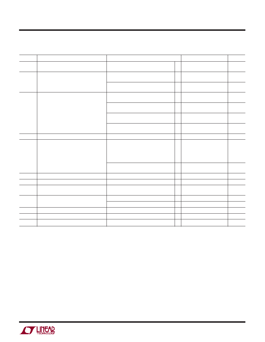
SYMBOL
PARAMETER
CONDITIONS
MIN
TYP
MAX
UNITS
ELECTRICAL CHARACTERISTICS
The q denotes the specifications which apply over the full specified temperature range, otherwise specifications are at TA = 25°C.
VCM = 0V, pulse tested, ±5V ≤ VS ≤ ±12V, VSHDNREF = 0V, RBIAS = 24.9k between V+ and SHDN unless otherwise noted. (Note 3)
PSRR
Power Supply Rejection Ratio
VS = ±4V to ±12V
74
88
dB
q
66
dB
AVOL
Large-Signal Voltage Gain
VS = ±12V, VOUT = ±10V, RL = 40
63
76
dB
q
57
dB
VS = ±5V, VOUT = ±3V, RL = 25
60
70
dB
q
54
dB
VOUT
Output Swing
VS = ±12V, RL = 100
10.9
11.1
±V
q
10.7
±V
VS = ±12V, IL = 250mA
10.6
10.9
±V
q
10.4
±V
VS = ±5V, RL = 25
3.7
4
±V
q
3.5
±V
VS = ±5V, IL = 250mA
3.6
3.9
±V
q
3.4
±V
IOUT
Maximum Output Current
VS = ±12V, RL = 1
500
1200
mA
IS
Supply Current per Amplifier
VS = ±12V, RBIAS = 24.9k (Note 7)
8.0
10
13.5
mA
q
6.7
15.0
mA
VS = ±12V, RBIAS = 32.4k (Note 7)
8
mA
VS = ±12V, RBIAS = 43.2k (Note 7)
6
mA
VS = ±12V, RBIAS = 66.5k (Note 7)
4
mA
VS = ±5V, RBIAS = 24.9k (Note 7)
2.2
3.4
5.0
mA
q
1.8
5.8
mA
Supply Current in Shutdown
VSHDN = 0.4V
0.1
1
mA
Output Leakage in Shutdown
VSHDN = 0.4V
0.3
1
mA
Channel Separation
VS = ±12V, VOUT = ±10V, RL = 40 (Note 8)
80
110
dB
q
77
dB
SR
Slew Rate
VS = ±12V, AV = – 10, (Note 9)
300
600
V/
s
VS = ±5V, AV = –10, (Note 9)
100
200
V/
s
HD2
Differential 2nd Harmonic Distortion
VS = ±12V, AV = 10, 2VP-P, RL = 50, 1MHz
– 85
dBc
HD3
Differential 3rd Harmonic Distortion
VS = ±12V, AV = 10, 2VP-P, RL = 50, 1MHz
– 82
dBc
GBW
Gain Bandwidth
f = 1MHz
200
MHz
Note 1: Absolute Maximum Ratings are those values beyond which the life
of a device may be impaired.
Note 2: Applies to short circuits to ground only. A short circuit between
the output and either supply may permanently damage the part when
operated on supplies greater than
±10V.
Note 3: The LT6301C is guaranteed to meet specified performance from
0
°C to 70°C and is designed, characterized and expected to meet these
extended temperature limits, but is not tested at – 40
°C and 85°C. The
LT6301I is guaranteed to meet the extended temperature limits.
Note 4: Thermal resistance varies depending upon the amount of PC board
metal attached to Pins 1, 14, 15, 28 and the exposed bottom side metal of
the device. If the maximum dissipation of the package is exceeded, the
device will go into thermal shutdown and be protected.
Note 5: Guaranteed by the CMRR tests.
Note 6: Matching is between amplifiers A and B or between amplifiers
C and D.
Note 7: RBIAS is connected between V
+ and each SHDN pin, with each
SHDNREF pin grounded.
Note 8: Channel separation is measured between amplifiers A and B and
between amplifiers C and D. Channel separation between any other
combination of amplifiers is guaranteed by design as two separate die are
used in the package.
Note 9: Slew rate is measured at
±5V on a ±10V output signal while
operating on
±12V supplies and ±1V on a ±3V output signal while
operating on
±5V supplies.
相关PDF资料 |
PDF描述 |
|---|---|
| LTC1346ACSW#PBF | IC TXRX V.35 DCE/DTE 24-SOIC |
| MS3106A18-19S | CONN PLUG 10POS STRAIGHT W/SCKT |
| LTC1350IG | IC TXRX 3.3V EIA/TIA-562 28-SSOP |
| IDT7207L25JI8 | IC FIFO 16384X18 25NS 32PLCC |
| VE-B6P-IV-F3 | CONVERTER MOD DC/DC 13.8V 150W |
相关代理商/技术参数 |
参数描述 |
|---|---|
| LT6301IFE | 功能描述:IC XDSL LINE DRIVER DUAL 28TSSOP RoHS:否 类别:集成电路 (IC) >> 接口 - 驱动器,接收器,收发器 系列:- 标准包装:250 系列:- 类型:收发器 驱动器/接收器数:2/2 规程:RS232 电源电压:3 V ~ 5.5 V 安装类型:表面贴装 封装/外壳:16-TSSOP(0.173",4.40mm 宽) 供应商设备封装:16-TSSOP 包装:带卷 (TR) |
| LT6301IFE#TR | 功能描述:IC XDSL LINE DRIVER DUAL 28TSSOP RoHS:否 类别:集成电路 (IC) >> 接口 - 驱动器,接收器,收发器 系列:- 标准包装:250 系列:- 类型:收发器 驱动器/接收器数:2/2 规程:RS232 电源电压:3 V ~ 5.5 V 安装类型:表面贴装 封装/外壳:16-TSSOP(0.173",4.40mm 宽) 供应商设备封装:16-TSSOP 包装:带卷 (TR) |
| LT6301IFE#TRPBF | 功能描述:IC XDSL LINE DRIVER DUAL 28TSSOP RoHS:是 类别:集成电路 (IC) >> 接口 - 驱动器,接收器,收发器 系列:- 标准包装:250 系列:- 类型:收发器 驱动器/接收器数:2/2 规程:RS232 电源电压:3 V ~ 5.5 V 安装类型:表面贴装 封装/外壳:16-TSSOP(0.173",4.40mm 宽) 供应商设备封装:16-TSSOP 包装:带卷 (TR) |
| LT630Z | 制造商:SEOUL 制造商全称:Seoul Semiconductor 功能描述:GREEN OVAL LAMP LED |
| LT631 | 制造商:SEOUL 制造商全称:Seoul Semiconductor 功能描述:BLUE OVAL LAMP LED |
发布紧急采购,3分钟左右您将得到回复。