- 您现在的位置:买卖IC网 > PDF目录39400 > LT6350HDD#PBF (LINEAR TECHNOLOGY CORP) 1-CH 16-BIT SUCCESSIVE APPROXIMATION ADC, PARALLEL ACCESS, PDSO8 PDF资料下载
参数资料
| 型号: | LT6350HDD#PBF |
| 厂商: | LINEAR TECHNOLOGY CORP |
| 元件分类: | ADC |
| 英文描述: | 1-CH 16-BIT SUCCESSIVE APPROXIMATION ADC, PARALLEL ACCESS, PDSO8 |
| 封装: | 3 X 3 MM, LEAD FREE, PLASTIC, MO-229WEED-1, DFN-8 |
| 文件页数: | 10/28页 |
| 文件大小: | 462K |
| 代理商: | LT6350HDD#PBF |
第1页第2页第3页第4页第5页第6页第7页第8页第9页当前第10页第11页第12页第13页第14页第15页第16页第17页第18页第19页第20页第21页第22页第23页第24页第25页第26页第27页第28页
LT6350
18
6350fb
–
+
–
+
–
+
–
RS
RG
R+IN2
RF
RINT
VOSOUT1
VOSOUT2
VOS1
VOS2
–IN1
+IN1
+IN2
OP AMP 1
OP AMP 2
6350 F07
IB1 +
IOS1
2
IB1 –
IOS1
2
IB2 –
IOS2
2
IB2 +
IOS2
2
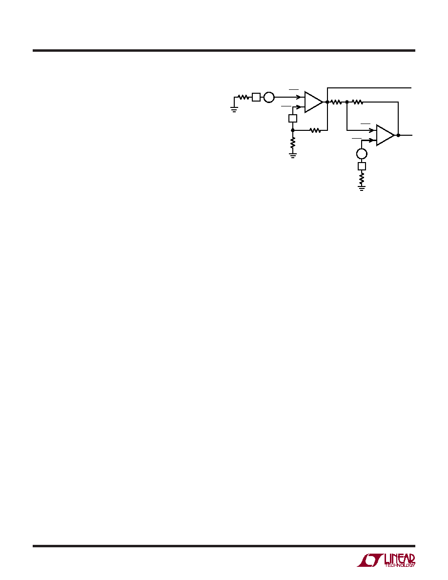
Figure 7. Offset Model
APPLICATIONS INFORMATION
In shutdown, all biasing current sources are shut off,
and the output pins, OUT1 and OUT2, each appear as
open collectors with non-linear capacitors in parallel and
steering diodes to either supply. Because of the non-linear
capacitance, the outputs still have the ability to sink and
source small amounts of transient current if driven with
signicant voltage transients. The input protection diodes
between +IN1 and +IN2 can still conduct if voltage tran-
sients at the input exceed 700mV. All other inputs also
have ESD protection diodes that can conduct when the
applied voltage exceeds 700mV. Using the SHDN feature
to wire-OR outputs together is not recommended.
The turn-on and turn off times between the shutdown and
active states are typically 400ns.
ESD
The LT6350 has ESD protection diodes on all inputs and
outputs. The diodes are reverse biased during normal
operation. If input pins are driven beyond either supply,
large currents will ow through these diodes. If the current
is transient and limited to 100mA or less, no damage to
the device will occur.
OFFSET CONSIDERATIONS
For excellent offset and distortion performance, both the
common mode and differential mode output voltage off-
sets are trimmed during manufacturing.
Figure 7 shows the contributors to DC offset voltage in
the LT6350.
The resulting DC offset voltages at pin OUT1 and OUT2
can be calculated:
VOSOUT1 = VOS1(1+RF/RG) + IB1(RF-RS(1+RF/RG))
– (IOS1/2)(RF+RS(1+RF/RG))
VOSOUT2 = –VOSOUT1 + 2VOS2 + IB2(RINT–2R+IN2)
– (IOS2/2)(RINT + 2R+IN2)
Using the above equations and Equations (2) and (3), the
output common mode and output differential mode offsets
can be found. The common mode offset is found to be:
VOSCM = VOS2 + IB2((RINT/2) – R+IN2) – (IOS2/2)
((RINT/2) + R+IN2)
相关PDF资料 |
PDF描述 |
|---|---|
| LT6350HMS8#PBF | 1-CH 16-BIT SUCCESSIVE APPROXIMATION ADC, PARALLEL ACCESS, PDSO8 |
| LT6350CDD#PBF | 1-CH 16-BIT SUCCESSIVE APPROXIMATION ADC, PARALLEL ACCESS, PDSO8 |
| LT6604IUFF-15#TRPBF | SPECIALTY ANALOG CIRCUIT, PQCC34 |
| LT6604IUFF-15#PBF | SPECIALTY ANALOG CIRCUIT, PQCC34 |
| LTC1093AMJ | 6-CH 10-BIT SUCCESSIVE APPROXIMATION ADC, SERIAL ACCESS, CDIP16 |
相关代理商/技术参数 |
参数描述 |
|---|---|
| LT6350HDDTRPBF | 制造商:LINER 制造商全称:Linear Technology 功能描述:Low Noise Single-Ended to Differential Converter/ADC Driver |
| LT6350HMS8#PBF | 功能描述:IC DIFF CONVERT/ADC DRIVER 8MSOP RoHS:是 类别:集成电路 (IC) >> 线性 - 放大器 - 专用 系列:- 产品培训模块:Lead (SnPb) Finish for COTS Obsolescence Mitigation Program 标准包装:60 系列:- 类型:可变增益放大器 应用:CATV 安装类型:表面贴装 封装/外壳:20-WQFN 裸露焊盘 供应商设备封装:20-TQFN-EP(5x5) 包装:托盘 |
| LT6350HMS8#TRPBF | 功能描述:IC DIFF CONVERT/ADC DRIVER 8MSOP RoHS:是 类别:集成电路 (IC) >> 线性 - 放大器 - 专用 系列:- 产品培训模块:Lead (SnPb) Finish for COTS Obsolescence Mitigation Program 标准包装:60 系列:- 类型:可变增益放大器 应用:CATV 安装类型:表面贴装 封装/外壳:20-WQFN 裸露焊盘 供应商设备封装:20-TQFN-EP(5x5) 包装:托盘 |
| LT6350HMS8PBF | 制造商:LINER 制造商全称:Linear Technology 功能描述:Low Noise Single-Ended to Differential Converter/ADC Driver |
| LT6350HMS8TRPBF | 制造商:LINER 制造商全称:Linear Technology 功能描述:Low Noise Single-Ended to Differential Converter/ADC Driver |
发布紧急采购,3分钟左右您将得到回复。