- 您现在的位置:买卖IC网 > PDF目录2156 > LT6600CS8-15#TRPBF (Linear Technology)IC AMP DIFF LP FLTR 15MHZ 8-SOIC PDF资料下载
参数资料
| 型号: | LT6600CS8-15#TRPBF |
| 厂商: | Linear Technology |
| 文件页数: | 12/12页 |
| 文件大小: | 0K |
| 描述: | IC AMP DIFF LP FLTR 15MHZ 8-SOIC |
| 标准包装: | 2,500 |
| 放大器类型: | 差分 |
| 电路数: | 1 |
| 输出类型: | 差分 |
| 电流 - 输入偏压: | 35µA |
| 电压 - 输入偏移: | 10000µV |
| 电流 - 电源: | 38mA |
| 电压 - 电源,单路/双路(±): | 3 V ~ 11 V,±1.5 V ~ 5.5 V |
| 工作温度: | 0°C ~ 70°C |
| 安装类型: | 表面贴装 |
| 封装/外壳: | 8-SOIC(0.154",3.90mm 宽) |
| 供应商设备封装: | 8-SO |
| 包装: | 带卷 (TR) |
LT6600-15
9
660015fb
APPLICATIONS INFORMATION
supply rails, the input/output behavior of the IC shown
in Figure 6 is relatively independent of the power supply
voltage.
The two ampliers inside the LT6600-15 have indepen-
dent control of their output common mode voltage (see
the Block Diagram section). The following guidelines will
optimize the performance of the lter.
Pin 7 must be bypassed to an AC ground with a 0.01μF or
larger capacitor. Pin 7 can be driven from a low impedance
source, provided it remains at least 1.5V above V– and at
least 1.5V below V+. An internal resistor divider sets the
voltage of Pin 7. While the internal 11k resistors are well
matched, their absolute value can vary by ±20%. This
should be taken into consideration when connecting an
external resistor network to alter the voltage of Pin 7.
Pin 2 can be shorted to Pin 7 for simplicity. If a different
common mode output voltage is required, connect Pin 2
to a voltage source or resistor network. For 3V and 3.3V
supplies the voltage at Pin 2 must be less than or equal to
the mid supply level. For example, voltage (Pin 2) ≤ 1.65V
on a single 3.3V supply. For power supply voltages higher
than 3.3V the voltage at Pin 2 should be within the voltage
of Pin 7 – 1V to the voltage of Pin 7 + 2V. Pin 2 is a high
impedance input.
The LT6600-15 was designed to process a variety of input
signals including signals centered around the mid-sup-
ply voltage and signals that swing between ground and
a positive voltage in a single supply system (Figure 1).
The range of allowable input common mode voltage (the
average of VIN+ and VIN– in Figure 1) is determined by
the power supply level and gain setting (see Distortion vs
Input Common Mode Level in the Typical Performance
Characteristics section).
Common Mode DC Currents
In applications like Figure 1 and Figure 3 where the
LT6600-15 not only provides lowpass ltering but also level
shifts the common mode voltage of the input signal, DC
currents will be generated through the DC path between
input and output terminals. Minimize these currents to
decrease power dissipation and distortion.
Consider the application in Figure 3. Pin 7 sets the output
common mode voltage of the 1st differential amplier
inside the LT6600-15 (see the Block Diagram section) at
2.5V. Since the input common mode voltage is near 0V, there
will be approximately a total of 2.5V drop across the series
combination of the internal 536Ω feedback resistor and the
external 133Ω input resistor. The resulting 3.7mA common
mode DC current in each input path, must be absorbed by
the sources VIN+ and VIN–. Pin 2 sets the common mode
output voltage of the 2nd differential amplier inside the
LT6600-15, and therefore sets the common mode output
voltage of the lter. Since, in the example of Figure 3, Pin 2
differs from Pin 7 by 0.5V, an additional 2.5mA (1.25mA
per side) of DC current will ow in the resistors coupling
the 1st differential amplier output stage to lter output.
Thus, a total of 9.9mA is used to translate the common
mode voltages.
A simple modication to Figure 3 will reduce the DC com-
mon mode currents by 40%. If Pin 7 is shorted to Pin 2
the common mode output voltage of both op amp stages
will be 2V and the resulting DC current will be 6mA. Of
course, by AC coupling the inputs of Figure 3, the common
mode DC current can be reduced to 2.5mA.
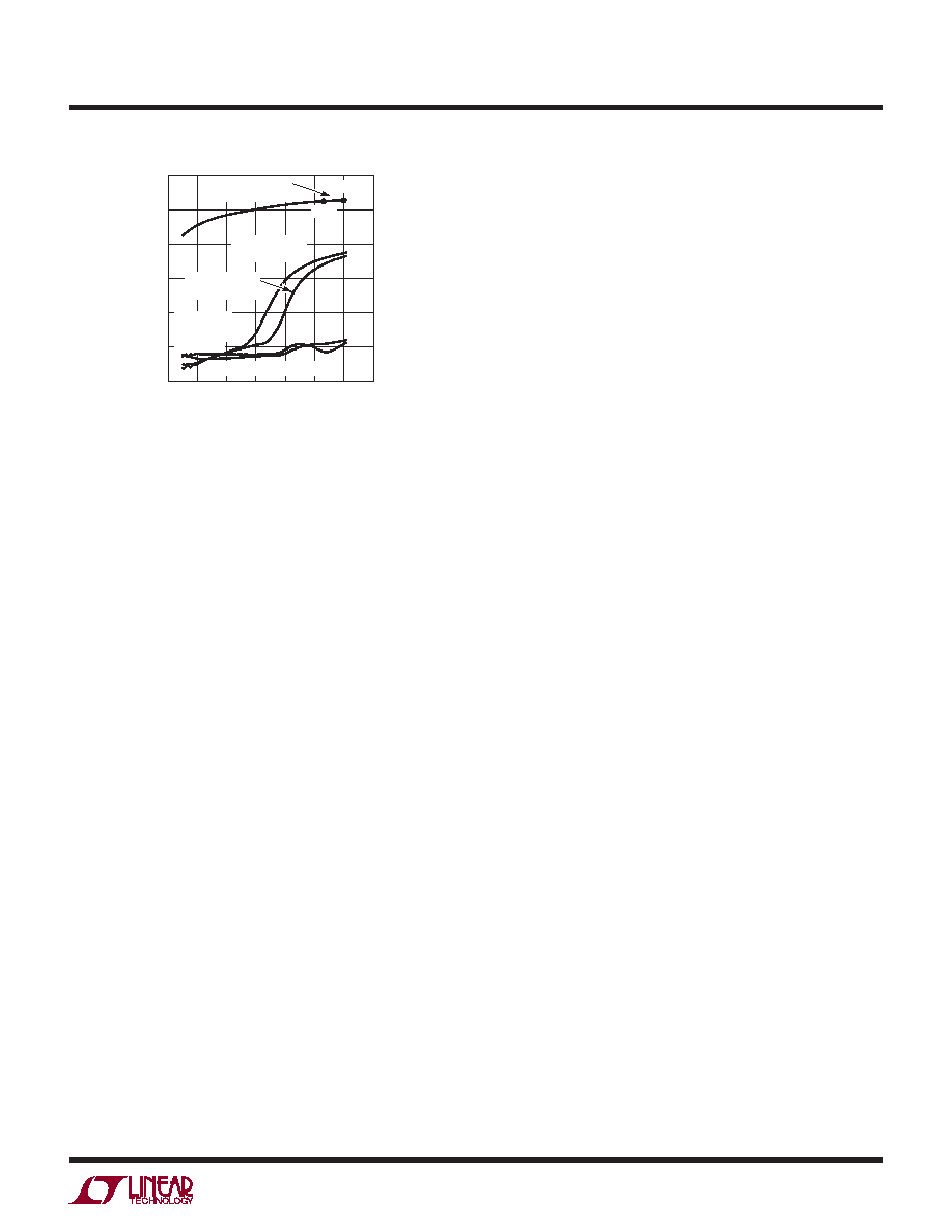
Figure 6. Output Level vs Input Level,
Differential 1MHz Input, Gain = 1
1MHz INPUT LEVEL (VP-P)
0
20
0
–20
–40
–60
–80
–100
35
660015 F06
12
46
7
OUTPUT
LEVEL
(dBV)
3RD HARMONIC
85°C
1dB COMPRESSION
POINTS
25°C
85°C
3RD HARMONIC
25°C
2ND HARMONIC, 25°C
2ND
HARMONIC
85°C
相关PDF资料 |
PDF描述 |
|---|---|
| LT6600CS8-5#TRPBF | IC AMP DIFF LP FLTR 5MHZ 8-SOIC |
| LT6600IS8-10 | IC AMP DIFF 10MHZ LP FLTR 8-SOIC |
| LT6600IS8-2.5#PBF | IC AMP DIFF LP FLTR 2.5MHZ 8SOIC |
| LT6600IS8-20 | IC AMP DIFF LP FLTR 20MHZ 8-SOIC |
| LT6604IUFF-2.5#TRPBF | IC AMP DIFF LN DUAL 34-QFN |
相关代理商/技术参数 |
参数描述 |
|---|---|
| LT6600CS8-2.5 | 功能描述:IC AMP DIFF LP FLTR 2.5MHZ 8SOIC RoHS:否 类别:集成电路 (IC) >> Linear - Amplifiers - Instrumentation 系列:- 标准包装:1 系列:- 放大器类型:通用 电路数:4 输出类型:满摆幅 转换速率:0.028 V/µs 增益带宽积:105kHz -3db带宽:- 电流 - 输入偏压:3nA 电压 - 输入偏移:100µV 电流 - 电源:3.3µA 电流 - 输出 / 通道:12mA 电压 - 电源,单路/双路(±):2.7 V ~ 12 V,±1.35 V ~ 6 V 工作温度:-40°C ~ 85°C 安装类型:表面贴装 封装/外壳:14-TSSOP(0.173",4.40mm 宽) 供应商设备封装:14-TSSOP 包装:剪切带 (CT) 其它名称:OP481GRUZ-REELCT |
| LT6600CS8-2.5#PBF | 功能描述:IC AMP DIFF LP FLTR 2.5MHZ 8SOIC RoHS:是 类别:集成电路 (IC) >> Linear - Amplifiers - Instrumentation 系列:- 标准包装:1 系列:- 放大器类型:通用 电路数:4 输出类型:满摆幅 转换速率:0.028 V/µs 增益带宽积:105kHz -3db带宽:- 电流 - 输入偏压:3nA 电压 - 输入偏移:100µV 电流 - 电源:3.3µA 电流 - 输出 / 通道:12mA 电压 - 电源,单路/双路(±):2.7 V ~ 12 V,±1.35 V ~ 6 V 工作温度:-40°C ~ 85°C 安装类型:表面贴装 封装/外壳:14-TSSOP(0.173",4.40mm 宽) 供应商设备封装:14-TSSOP 包装:剪切带 (CT) 其它名称:OP481GRUZ-REELCT |
| LT6600CS8-2.5#TR | 功能描述:IC AMP DIFF LP FLTR 2.5MHZ 8SOIC RoHS:否 类别:集成电路 (IC) >> Linear - Amplifiers - Instrumentation 系列:- 标准包装:50 系列:- 放大器类型:J-FET 电路数:2 输出类型:- 转换速率:3.5 V/µs 增益带宽积:1MHz -3db带宽:- 电流 - 输入偏压:30pA 电压 - 输入偏移:2000µV 电流 - 电源:200µA 电流 - 输出 / 通道:- 电压 - 电源,单路/双路(±):7 V ~ 36 V,±3.5 V ~ 18 V 工作温度:0°C ~ 70°C 安装类型:通孔 封装/外壳:8-DIP(0.300",7.62mm) 供应商设备封装:8-PDIP 包装:管件 |
| LT6600CS8-2.5#TRPBF | 功能描述:IC AMP DIFF LP FLTR 2.5MHZ 8SOIC RoHS:是 类别:集成电路 (IC) >> Linear - Amplifiers - Instrumentation 系列:- 标准包装:50 系列:- 放大器类型:J-FET 电路数:2 输出类型:- 转换速率:3.5 V/µs 增益带宽积:1MHz -3db带宽:- 电流 - 输入偏压:30pA 电压 - 输入偏移:2000µV 电流 - 电源:200µA 电流 - 输出 / 通道:- 电压 - 电源,单路/双路(±):7 V ~ 36 V,±3.5 V ~ 18 V 工作温度:0°C ~ 70°C 安装类型:通孔 封装/外壳:8-DIP(0.300",7.62mm) 供应商设备封装:8-PDIP 包装:管件 |
| LT6600CS8-2.5-PBF | 制造商:LINER 制造商全称:Linear Technology 功能描述:Very Low Noise, Differential Amplifi er and 2.5MHz Lowpass Filter |
发布紧急采购,3分钟左右您将得到回复。