- 您现在的位置:买卖IC网 > PDF目录44987 > LT6660HCDC-10#PBF (LINEAR TECHNOLOGY CORP) 1-OUTPUT THREE TERM VOLTAGE REFERENCE, 10 V, PSSO3 PDF资料下载
参数资料
| 型号: | LT6660HCDC-10#PBF |
| 厂商: | LINEAR TECHNOLOGY CORP |
| 元件分类: | 基准电压源/电流源 |
| 英文描述: | 1-OUTPUT THREE TERM VOLTAGE REFERENCE, 10 V, PSSO3 |
| 封装: | 2 X 2 MM, 0.75 MM, LEAD FREE, PLASTIC, MO-229W-TBD, DFN-3 |
| 文件页数: | 11/12页 |
| 文件大小: | 400K |
| 代理商: | LT6660HCDC-10#PBF |
LT6660
8
6660fa
APPLICATIO S I FOR ATIO
W
U
Longer Battery Life
Series references have a large advantage over older shunt
style references. Shunt references require a resistor
from the power supply to operate. This resistor must be
chosen to supply the maximum current that can ever be
demanded by the circuit being regulated. When the circuit
being controlled is not operating at this maximum current,
theshuntreferencemustalwayssinkthiscurrent,resulting
in high dissipation and short battery life.
The LT6660 series references do not require a current
setting resistor and can operate with any supply voltage
from VOUT + 0.9V to 20V. When the circuitry being regu-
lated does not demand current, the LT6660s reduce their
dissipation and battery life is extended. If the references
are not delivering load current, they dissipate only several
mW, yet the same connection can deliver 20mA of load
current when demanded.
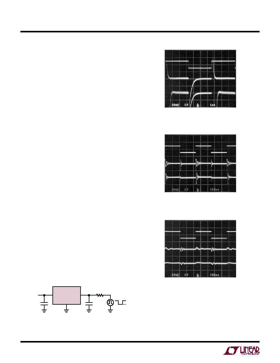
Capacitive Loads
The LT6660 family of references are designed to be stable
with a large range of capacitive loads. With no capacitive
load, these references are ideal for fast settling or applica-
tions where PC board space is a premium. The test circuit
shown in Figure 1 is used to measure the response time
and stability of various load currents and load capacitors.
This circuit is set for the 2.5V option. For other voltage
options, the input voltage must be scaled up and the
output voltage generator offset voltage must be adjusted.
The 1V step from 2.5V to 1.5V produces a current step of
10mA or 1mA for RL = 100Ω or RL = 1k. Figure 2 shows
the response of the reference to these 1mA and 10mA
load steps with no load capacitance, and Figure 3 shows
a 1mA and 10mA load step with a 0.1F output capaci-
tor. Figure 4 shows the response to a 1mA load step with
CL = 1F and 4.7F.
Figure 2. CL = 0F
Figure 3. CL = 0.1F
Figure 4. IOUT = 1mA
1
s/DIV
VGEN
VOUT
2.5V
1.5V
1mA
10mA
6660 F02
100
s/DIV
VGEN
VOUT
2.5V
1.5V
1mA
10mA
6660 F03
100
s/DIV
VGEN
VOUT
2.5V
1.5V
1
F
4.7
F
6660 F04
Figure 1. Response Time Test Circuit
LT6660-2.5
RL
VOUT
VGEN
6660 F01
CIN
0.1
F
2.5V
1.5V
CL
VIN = 2.5V
相关PDF资料 |
PDF描述 |
|---|---|
| LT6660JCDC-10#TRPBF | 1-OUTPUT THREE TERM VOLTAGE REFERENCE, 10 V, PSSO3 |
| LT8415IDDB#PBF | 0.03 A SWITCHING REGULATOR, PDSO12 |
| LT8415EDDB#TRMPBF | 0.03 A SWITCHING REGULATOR, PDSO12 |
| LT8415IDDB#TRPBF | 0.03 A SWITCHING REGULATOR, PDSO12 |
| LTC1043MD/883B | SPECIALTY ANALOG CIRCUIT, CDIP18 |
相关代理商/技术参数 |
参数描述 |
|---|---|
| LT6660HCDC-2.5 | 制造商:LINER 制造商全称:Linear Technology 功能描述:Tiny Micropower Precision Series References in 2mm × 2mm DFN |
| LT6660HCDC-2.5#PBF | 制造商:Linear Technology 功能描述:IC SM VOLT REF 2.5V 制造商:Linear Technology 功能描述:IC, SM, VOLT REF, 2.5V |
| LT6660HCDC-2.5#TR | 制造商:Linear Technology 功能描述:SC-Refs/Series, 2.5V Low Cost uP Prec Series Ref. |
| LT6660HCDC-2.5#TRMPBF | 功能描述:IC VREF SERIES PREC 2.5V 3-DFN RoHS:是 类别:集成电路 (IC) >> PMIC - 电压基准 系列:- 标准包装:3,000 系列:- 基准类型:旁路,精度 输出电压:3V 容差:±0.5% 温度系数:100ppm/°C 输入电压:- 通道数:1 电流 - 阴极:82µA 电流 - 静态:- 电流 - 输出:15mA 工作温度:-40°C ~ 85°C 安装类型:表面贴装 封装/外壳:6-TSSOP(5 引线),SC-88A,SOT-353 供应商设备封装:SC-70-5 包装:带卷 (TR) 其它名称:296-20888-2 |
| LT6660HCDC-2.5#TRPBF | 功能描述:IC VREF SERIES PREC 2.5V 3-DFN RoHS:是 类别:集成电路 (IC) >> PMIC - 电压基准 系列:- 产品培训模块:Voltage Reference Basics 标准包装:100 系列:- 基准类型:旁路,精度 输出电压:4.096V 容差:±0.075% 温度系数:50ppm/°C 输入电压:- 通道数:1 电流 - 阴极:1µA 电流 - 静态:- 电流 - 输出:10mA 工作温度:0°C ~ 70°C 安装类型:表面贴装 封装/外壳:8-SOIC(0.154",3.90mm 宽) 供应商设备封装:8-SOIC 包装:管件 |
发布紧急采购,3分钟左右您将得到回复。