- 您现在的位置:买卖IC网 > PDF目录44988 > LT8415IDDB#TRPBF (LINEAR TECHNOLOGY CORP) 0.03 A SWITCHING REGULATOR, PDSO12 PDF资料下载
参数资料
| 型号: | LT8415IDDB#TRPBF |
| 厂商: | LINEAR TECHNOLOGY CORP |
| 元件分类: | 稳压器 |
| 英文描述: | 0.03 A SWITCHING REGULATOR, PDSO12 |
| 封装: | 3 X 2 MM, LEAD FREE, PLASTIC, DFN-12 |
| 文件页数: | 2/12页 |
| 文件大小: | 182K |
| 代理商: | LT8415IDDB#TRPBF |
LT8415
10
8415f
APPLICATIONS INFORMATION
If the application doesn’t require the output disconnect
function, the CAP and VOUT pin can be shorted, and higher
power converter efciency can be achieved.
SHDN Pin Comparator and Hysteresis Current
An internal comparator compares the SHDN pin voltage
with an internal voltage reference (~1.3V) which gives a
precise turn-on voltage level. The internal hysteresis of this
turn-on voltage is about 60mV. When the chip is turned on,
and the SHDN pin voltage is close to this turn-on voltage,
0.1μA current ows out of the SHDN pin. This current is
called SHDN pin hysteresis current, and will go away when
the chip is off. By connecting the external resistors as in
Figure 2, a user-programmable enable voltage function
can be realized.
The turn-on voltage for the conguration is:
1.30 (1 + R1/R2)
and the turn-off voltage is:
(1.24 – R3 10–7) (1 + R1/R2) – R1 10–7
where R1, R2 and R3 are resistance value in Ω.
R1
ENABLE VOLTAGE
R2
R3
CONNECT TO
SHDN PIN
Figure 2. Programming Enable Voltage by Using External
Resistors
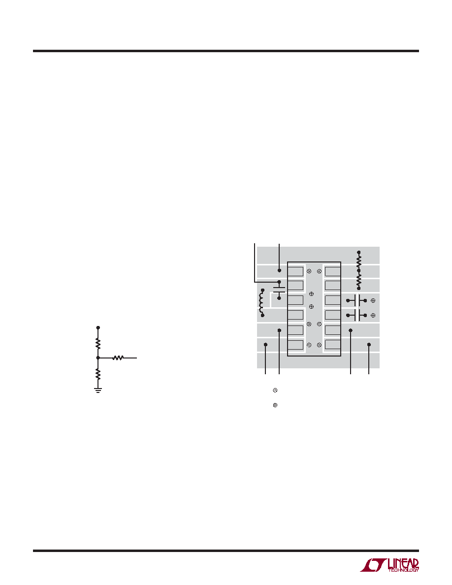
Board Layout Considerations
As with all switching regulators, careful attention must
be paid to the PCB layout and component placement. To
maximize efciency, switch rise and fall times are made
as short as possible. To prevent electromagnetic interfer-
ence (EMI) problems, proper layout of the high frequency
switching path is essential. The voltage signal of the SW pin
has sharp rising and falling edges. Minimize the length and
area of all traces connected to the SW pin and always use
a ground plane under the switching regulator to minimize
interplane coupling. In addition, the FBP pin and VREF pin
are sensitive to noise. Minimizing the length and area of all
traces to these two pins is recommended. Recommended
component placement is shown in Figure 3.
VIAS TO GROUND PLANE REQUIRED
TO IMPROVE THERMAL PERFORMANCE
VIAS FOR CAP AND VOUT GROUND RETURN THROUGH
SECOND METAL LAYER, CAPACITOR GROUNDS MUST
BE RETURNED DIRECTLY TO IC GROUND
8410 F03
SHDN
GND
SW
IN1
IN2
VCC
FBP
CAP
VREF
VOUT
OUT1
OUT2
GND
VIN
SHDN
IN2
IN1
OUT1
OUT2
Figure 3. Recommended Board Layout
Half-Bridge Control Signals
The half-bridge is controlled by the IN1 and IN2 pins. The
IN1 and IN2 pins should be driven with a logic signal.
When the chip is enabled, the OUT1 and OUT2 voltages
are equal to VOUT IN1 and IN2 are driven higher than 1V,
and they are near GND when IN1 and IN2 are driven below
0.3V. Do not drive the IN1 or IN2 pins between 0.3V to
1V for more than 20μs since this will leave OUT1 or OUT2
in an uncertain state and may also cause shoot-through
current.
相关PDF资料 |
PDF描述 |
|---|---|
| LTC1043MD/883B | SPECIALTY ANALOG CIRCUIT, CDIP18 |
| LTC1146ACN | SPECIALTY ANALOG CIRCUIT, PDIP18 |
| LTC1148HVCS-3.3#TR | SWITCHING CONTROLLER, 250 kHz SWITCHING FREQ-MAX, PDSO14 |
| LTC1148HVCS-5#TR | SWITCHING CONTROLLER, 250 kHz SWITCHING FREQ-MAX, PDSO14 |
| LTC1149CN-5#PBF | SWITCHING CONTROLLER, 250 kHz SWITCHING FREQ-MAX, PDIP16 |
相关代理商/技术参数 |
参数描述 |
|---|---|
| LT8500EUHH#PBF | 功能描述:IC PWM GENERATOR 56-QFN RoHS:是 类别:集成电路 (IC) >> 时钟/计时 - 专用 系列:- 标准包装:1 系列:- 类型:时钟/频率发生器,多路复用器 PLL:是 主要目的:存储器,RDRAM 输入:晶体 输出:LVCMOS 电路数:1 比率 - 输入:输出:1:2 差分 - 输入:输出:无/是 频率 - 最大:400MHz 电源电压:3 V ~ 3.6 V 工作温度:0°C ~ 85°C 安装类型:表面贴装 封装/外壳:16-TSSOP(0.173",4.40mm 宽) 供应商设备封装:16-TSSOP 包装:Digi-Reel® 其它名称:296-6719-6 |
| LT8500EUHH#TRPBF | 功能描述:IC PWM GENERATOR 56-QFN RoHS:是 类别:集成电路 (IC) >> 时钟/计时 - 专用 系列:- 标准包装:28 系列:- 类型:时钟/频率发生器 PLL:是 主要目的:Intel CPU 服务器 输入:时钟 输出:LVCMOS 电路数:1 比率 - 输入:输出:3:22 差分 - 输入:输出:无/是 频率 - 最大:400MHz 电源电压:3.135 V ~ 3.465 V 工作温度:0°C ~ 85°C 安装类型:表面贴装 封装/外壳:64-TFSOP (0.240",6.10mm 宽) 供应商设备封装:64-TSSOP 包装:管件 |
| LT8500IUHH#PBF | 功能描述:IC PWM GENERATOR 56-QFN RoHS:是 类别:集成电路 (IC) >> 时钟/计时 - 专用 系列:- 标准包装:28 系列:- 类型:时钟/频率发生器 PLL:是 主要目的:Intel CPU 服务器 输入:时钟 输出:LVCMOS 电路数:1 比率 - 输入:输出:3:22 差分 - 输入:输出:无/是 频率 - 最大:400MHz 电源电压:3.135 V ~ 3.465 V 工作温度:0°C ~ 85°C 安装类型:表面贴装 封装/外壳:64-TFSOP (0.240",6.10mm 宽) 供应商设备封装:64-TSSOP 包装:管件 |
| LT8500IUHH#TRPBF | 功能描述:IC PWM GENERATOR 56-QFN RoHS:是 类别:集成电路 (IC) >> 时钟/计时 - 专用 系列:- 标准包装:28 系列:- 类型:时钟/频率发生器 PLL:是 主要目的:Intel CPU 服务器 输入:时钟 输出:LVCMOS 电路数:1 比率 - 输入:输出:3:22 差分 - 输入:输出:无/是 频率 - 最大:400MHz 电源电压:3.135 V ~ 3.465 V 工作温度:0°C ~ 85°C 安装类型:表面贴装 封装/外壳:64-TFSOP (0.240",6.10mm 宽) 供应商设备封装:64-TSSOP 包装:管件 |
| LT-8501M | 制造商:Mencom 功能描述: |
发布紧急采购,3分钟左右您将得到回复。