- 您现在的位置:买卖IC网 > PDF目录8991 > LTC1045CN#PBF (Linear Technology)IC TRANSLATOR/RCVR/DVR HEX 20DIP PDF资料下载
参数资料
| 型号: | LTC1045CN#PBF |
| 厂商: | Linear Technology |
| 文件页数: | 18/20页 |
| 文件大小: | 0K |
| 描述: | IC TRANSLATOR/RCVR/DVR HEX 20DIP |
| 标准包装: | 18 |
| 逻辑功能: | 可编程变换器/接收器/驱动器,3 态 |
| 位数: | 6 |
| 输入类型: | CMOS/TTL |
| 输出类型: | TTL |
| 通道数: | 6 |
| 输出/通道数目: | 1 |
| 差分 - 输入:输出: | 无/无 |
| 传输延迟(最大): | 350ns |
| 电源电压: | 3 V ~ 15 V |
| 工作温度: | -40°C ~ 85°C |
| 封装/外壳: | 20-DIP(0.300",7.62mm) |
| 供应商设备封装: | 20-PDIP |
| 包装: | 管件 |
| 产品目录页面: | 1356 (CN2011-ZH PDF) |
7
LTC1045
1045fc
Because of this diode, VOH must not be greater than V +.
Lastly, the maximum voltage between any two power
supply pins must not exceed 15V operating or 18V abso-
lute maximum. For example, if V + = 5V, V – or VOL should
be no more negative than – 10V. Note that VOL should not
be more negative than – 10V even if the VOH to VOL
differential does not exceed the 15V maximum. In this
case the V + to VOL differential sets the limit.
Input Voltage
The LTC1045 has no upper clamp diodes as do conven-
tional CMOS circuits. This allows the inputs to exceed the
V + supply. The inputs will break down approximately 30V
above the V – supply. If the input current is limited with
100k
, the input voltage can be driven to at least ±50V
with no adverse effects for any combination of allowed
APPLICATIONS INFORMATION
WU
U
power supply voltages. Output levels will be correct even
under these conditions (i.e., if the input voltage is above
the trip point, the output will be high and if it is below, the
output will be low).
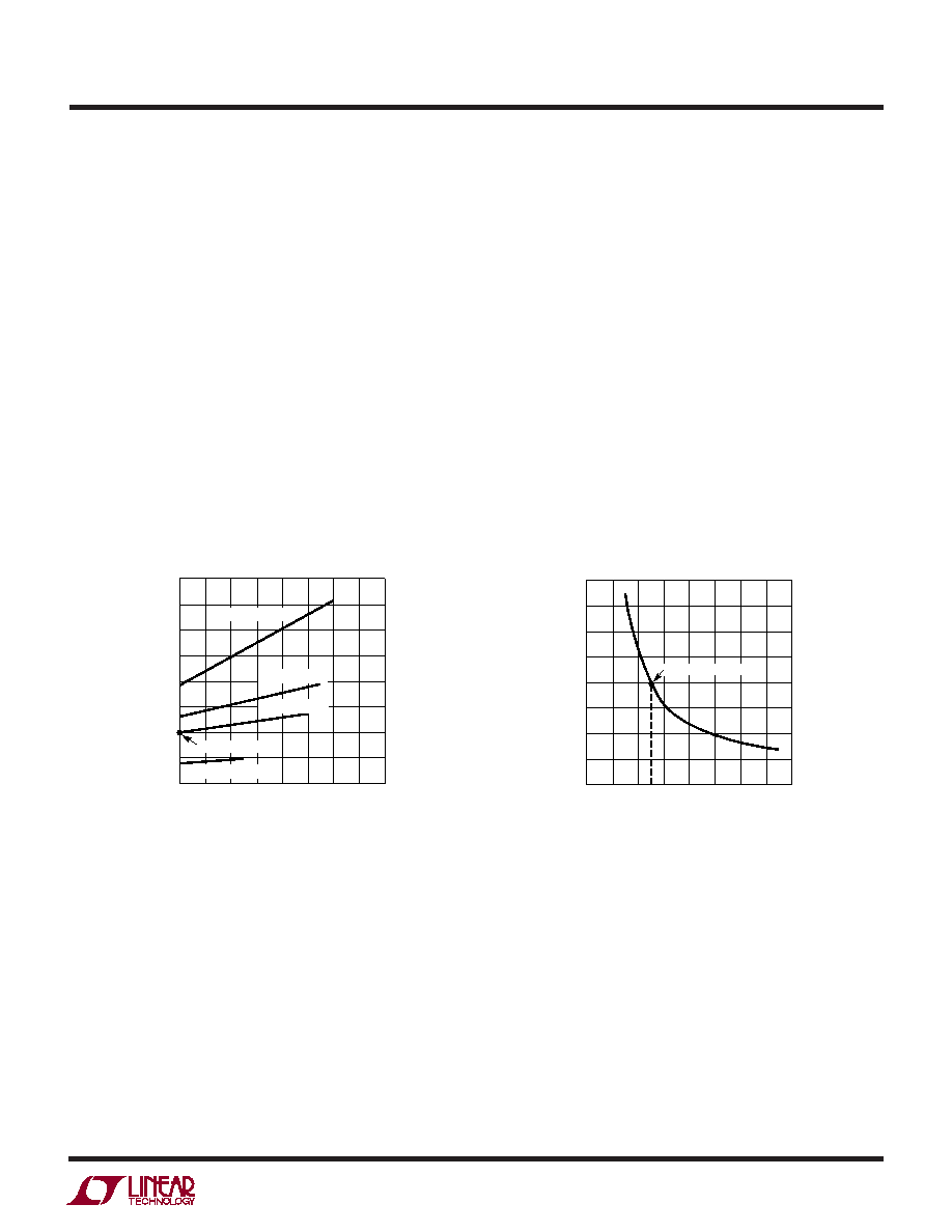
Output Drive
Output drive characteristics of the LTC1045 will vary with
the power supply voltages that are chosen. Output imped-
ance is affected by V +, VOH and VOL. V – has no effect on
output impedance. Guaranteed drive characteristics are
specified in the table of electrical characteristics for
V + = VOH = 5V and V – = VOL = 0V. Figures 6 and 7 show
relative output impedance for other supply combinations.
In general, output impedance is minimized if V + to VOH is
minimized and VOH to VOL is maximized.
V+ – VOH (V)
02
R
OH
/[
R
OH
AT
(V
OH
–
V
OL
)=
5V
AND
(V
+ –
V
OH
)=
0V]
16
1045 F06
4
6
10
14
8
12
4
3
2
1
0
SPECIFIED POINT
VOH – VOL = 5V
VOH – VOL = 10V
VOH – VOL = 4V
VOH – VOL = 3V
VOH – VOL (V)
02
R
OL
/[
R
OL
AT
(V
OH
–
V
OL
)=
5V]
16
1045 F07
4
6
10
14
8
12
2
1
0
SPECIFIED POINT
Figure 6. Relative Output Sourcing
Resistance (ROH) vs V + – VOH
Figure 7. Relative Output Sinking
Resistance (ROL) vs VOH – VOL
相关PDF资料 |
PDF描述 |
|---|---|
| VI-24D-MY-F3 | CONVERTER MOD DC/DC 85V 50W |
| LTC1555IGN#PBF | IC LEVEL TRANSLATOR 16-SSOP |
| ADG3308BRUZ | IC XLATOR 8CH 1.2-5.5V 20-TSSOP |
| MS27497T24F2SB | CONN RCPT 100POS WALL MNT W/SCKT |
| SY10ELT20VZG | IC TRANSLATOR PECL 3.3/5V 8-SOIC |
相关代理商/技术参数 |
参数描述 |
|---|---|
| LTC1045CSW | 功能描述:IC TRANSLATR/RCVR/DVR HEX 20SOIC RoHS:否 类别:集成电路 (IC) >> 逻辑 - 变换器 系列:- 产品培训模块:Logic Packages 标准包装:2,500 系列:- 逻辑功能:变换器,双向 位数:2 输入类型:电压 输出类型:电压 数据速率:- 通道数:2 输出/通道数目:1 差分 - 输入:输出:无/无 传输延迟(最大):1.5ns 电源电压:3 V ~ 3.6 V 工作温度:-40°C ~ 85°C 封装/外壳:8-TSSOP,8-MSOP(0.118",3.00mm 宽) 供应商设备封装:8-TSSOP 包装:带卷 (TR) 其它名称:935284857118GTL2002DP/S440-TGTL2002DP/S440-T-ND |
| LTC1045CSW#PBF | 功能描述:IC TRANSLATR/RCVR/DVR HEX 20SOIC RoHS:是 类别:集成电路 (IC) >> 逻辑 - 变换器 系列:- 产品培训模块:Logic Packages 标准包装:2,500 系列:- 逻辑功能:变换器,双向 位数:2 输入类型:电压 输出类型:电压 数据速率:- 通道数:2 输出/通道数目:1 差分 - 输入:输出:无/无 传输延迟(最大):1.5ns 电源电压:3 V ~ 3.6 V 工作温度:-40°C ~ 85°C 封装/外壳:8-TSSOP,8-MSOP(0.118",3.00mm 宽) 供应商设备封装:8-TSSOP 包装:带卷 (TR) 其它名称:935284857118GTL2002DP/S440-TGTL2002DP/S440-T-ND |
| LTC1045CSW#TR | 功能描述:IC TRANSLATOR HEX UNIV 20SOIC RoHS:否 类别:集成电路 (IC) >> 逻辑 - 变换器 系列:- 产品培训模块:Logic Packages 标准包装:2,500 系列:- 逻辑功能:变换器,双向 位数:2 输入类型:电压 输出类型:电压 数据速率:- 通道数:2 输出/通道数目:1 差分 - 输入:输出:无/无 传输延迟(最大):1.5ns 电源电压:3 V ~ 3.6 V 工作温度:-40°C ~ 85°C 封装/外壳:8-TSSOP,8-MSOP(0.118",3.00mm 宽) 供应商设备封装:8-TSSOP 包装:带卷 (TR) 其它名称:935284857118GTL2002DP/S440-TGTL2002DP/S440-T-ND |
| LTC1045CSW#TRPBF | 功能描述:IC TRANSLATR/RCVR/DVR HEX 20SOIC RoHS:是 类别:集成电路 (IC) >> 逻辑 - 变换器 系列:- 产品培训模块:Logic Packages 标准包装:2,500 系列:- 逻辑功能:变换器,双向 位数:2 输入类型:电压 输出类型:电压 数据速率:- 通道数:2 输出/通道数目:1 差分 - 输入:输出:无/无 传输延迟(最大):1.5ns 电源电压:3 V ~ 3.6 V 工作温度:-40°C ~ 85°C 封装/外壳:8-TSSOP,8-MSOP(0.118",3.00mm 宽) 供应商设备封装:8-TSSOP 包装:带卷 (TR) 其它名称:935284857118GTL2002DP/S440-TGTL2002DP/S440-T-ND |
| LTC1046 | 制造商:LINER 制造商全称:Linear Technology 功能描述:“Inductorless” 5V to + 5V Converter |
发布紧急采购,3分钟左右您将得到回复。