参数资料
| 型号: | LTC1052CN#PBF |
| 厂商: | Linear Technology |
| 文件页数: | 3/24页 |
| 文件大小: | 0K |
| 描述: | IC OPAMP CHOP-STBL LONOIS 14DIP |
| 标准包装: | 25 |
| 系列: | LTCMOS™ |
| 放大器类型: | 断路器(零漂移) |
| 电路数: | 1 |
| 转换速率: | 4 V/µs |
| 增益带宽积: | 1.2MHz |
| 电流 - 输入偏压: | 1pA |
| 电压 - 输入偏移: | 0.5µV |
| 电流 - 电源: | 1.7mA |
| 电压 - 电源,单路/双路(±): | 4.75 V ~ 16 V,±2.38 V ~ 8 V |
| 工作温度: | 0°C ~ 70°C |
| 安装类型: | 通孔 |
| 封装/外壳: | 14-DIP(0.300",7.62mm) |
| 供应商设备封装: | 14-PDIP |
| 包装: | 管件 |
| 产品目录页面: | 1321 (CN2011-ZH PDF) |
LTC1052/LTC7652
11
1052fa
PACKAGE-INDUCED OFFSET VOLTAGE
Since the LTC1052 is constantly fixing its own offset, it
may be asked why there is any error at all, even under
transient temperature conditions. The answer is simple.
The LTC1052 can only fix offsets inside its own nulling
loop. There are many thermal junctions outside this loop
that cannot be distinguished from legitimate signals.
Some have been discussed previously, but the package
thermal EMF effects are an important source of errors.
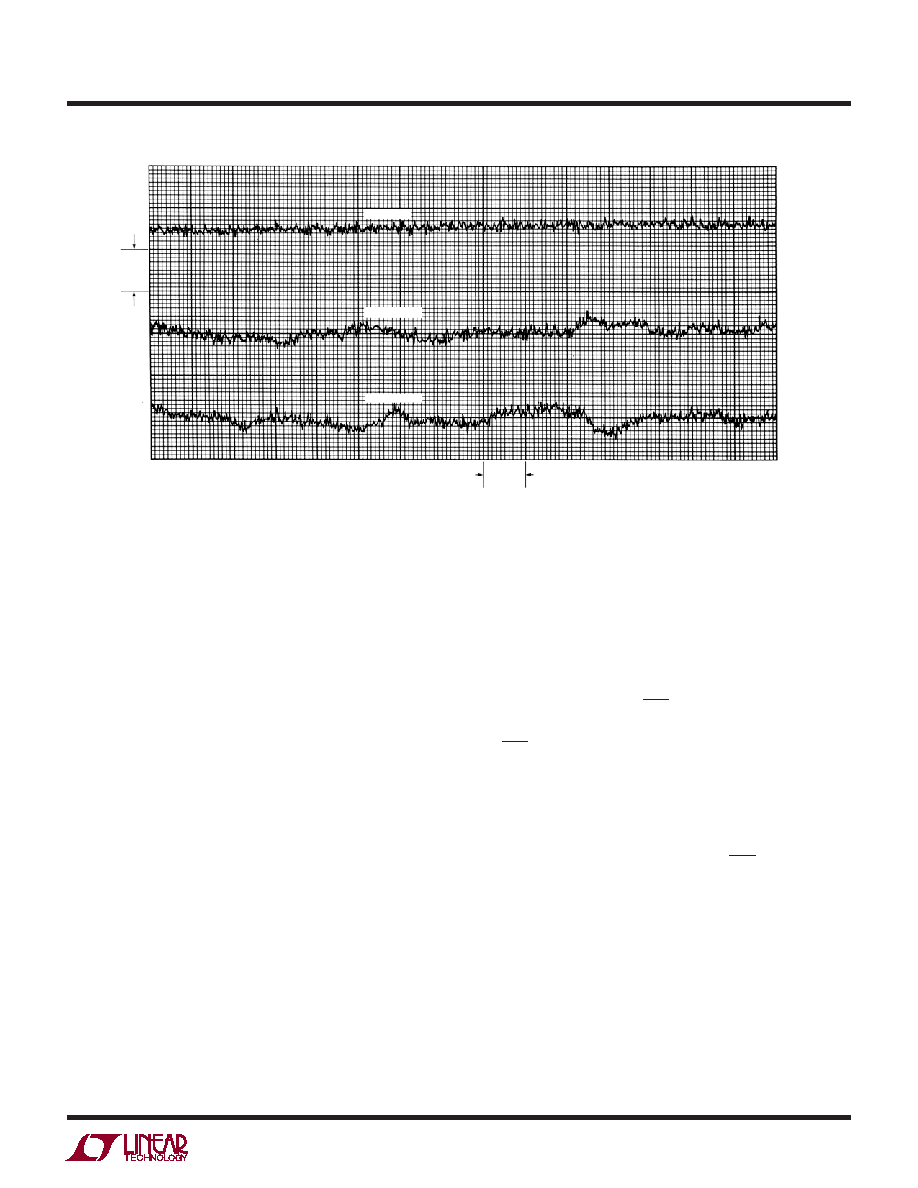
Notice the difference in the thermal response curves of
Figure 4. This can only be attributed to the package since
everything else is identical. In fact, the VOS specification is
set by the package-induced warm-up drift, not by the
LTC1052. TO-99 metal cans exhibit the worst warm-up
drift and Linear Technology sample tests TO-99 lots to
minimize this problem.
Two things make 100% screening costly: (1) The extreme
precision required on the LTC1052 and (2) the thermal
time constant of the package is 0.5 to 3 minutes, depend-
ing on package type. The first precludes the use of auto-
matic handling equipment and the second takes a long
time. Bench test equipment is available to 100% test for
warmed-up drift if offsets of less than ±5V are required.
APPLICATIO S I FOR ATIO
WU
UU
Figure 5. DC to 1Hz (Test Circuit TC3)
1V
#1 COVERED
#1 UNCOVERED
#2 UNCOVERED
20 SEC
CLOCK
The LTC1052 has an internal clock, setting the nominal
sampling frequency at 330Hz. On 8-pin devices, there is
no way to control the clock externally. In some applica-
tions it may be desirable to control the sampling clock and
this is the function of the 14-pin device.
CLK IN, CLK OUT and INT/EXT are provided to accomplish
this. With no external connection, an internal pull-up holds
INT/EXT at the V+ supply and the 14-pin device self-
oscillates at 330Hz. In this mode there is a signal on the
CLK IN pin of 660Hz (2 times sampling frequency) with a
30% duty cycle. A divide-by-two drives the CLK OUT pin
and sets the sampling frequency.
To use an external clock, connect INT/EXT to V– and the
external clock to CLK IN. The logic threshold of CLK IN is
2.5V below the positive supply; this allows CMOS logic to
drive it directly with logic supplies of V+ and ground. CLK
IN can be driven from V+ to V– if desired. The duty cycle of
the external clock is not particularly critical but should be
kept between 30% and 60%.
Capacitance between CLK IN and CLK OUT (pins 13 and
12) can cause the divide-by-two circuit to malfunction. To
avoid this, keep this capacitance below 5pF.
相关PDF资料 |
PDF描述 |
|---|---|
| ADA4610-2BRZ | IC OPAMP JFET R-R DUAL 8SOIC |
| OP462GSZ | IC OPAMP GP R-R 15MHZ LN 14SOIC |
| LT1114S#PBF | IC PREC OP-AMP LOPWR QUAD 16SOIC |
| LTC1150CS8#PBF | IC OPAMP CHOP-STBL W/CAPS 8SOIC |
| LT1079SW#PBF | IC PREC OP-AMP MCRPWR QUAD16SOIC |
相关代理商/技术参数 |
参数描述 |
|---|---|
| LTC1052CS | 制造商:LINTEC 功能描述: |
| LTC1052CSW | 功能描述:IC OPAMP CHOP-STBL LONOIS16SOIC RoHS:否 类别:集成电路 (IC) >> Linear - Amplifiers - Instrumentation 系列:LTCMOS™ 标准包装:150 系列:- 放大器类型:音频 电路数:2 输出类型:- 转换速率:5 V/µs 增益带宽积:12MHz -3db带宽:- 电流 - 输入偏压:100nA 电压 - 输入偏移:500µV 电流 - 电源:6mA 电流 - 输出 / 通道:50mA 电压 - 电源,单路/双路(±):4 V ~ 32 V,±2 V ~ 16 V 工作温度:-40°C ~ 85°C 安装类型:表面贴装 封装/外壳:8-TSSOP(0.173",4.40mm 宽) 供应商设备封装:8-TSSOP 包装:管件 |
| LTC1052CSW#PBF | 功能描述:IC OPAMP CHOP-STBL LONOIS16SOIC RoHS:是 类别:集成电路 (IC) >> Linear - Amplifiers - Instrumentation 系列:LTCMOS™ 标准包装:150 系列:- 放大器类型:音频 电路数:2 输出类型:- 转换速率:5 V/µs 增益带宽积:12MHz -3db带宽:- 电流 - 输入偏压:100nA 电压 - 输入偏移:500µV 电流 - 电源:6mA 电流 - 输出 / 通道:50mA 电压 - 电源,单路/双路(±):4 V ~ 32 V,±2 V ~ 16 V 工作温度:-40°C ~ 85°C 安装类型:表面贴装 封装/外壳:8-TSSOP(0.173",4.40mm 宽) 供应商设备封装:8-TSSOP 包装:管件 |
| LTC1052CSW#TR | 功能描述:IC OPAMP CHOP STABLE LN 16SOIC RoHS:否 类别:集成电路 (IC) >> Linear - Amplifiers - Instrumentation 系列:LTCMOS™ 标准包装:150 系列:- 放大器类型:音频 电路数:2 输出类型:- 转换速率:5 V/µs 增益带宽积:12MHz -3db带宽:- 电流 - 输入偏压:100nA 电压 - 输入偏移:500µV 电流 - 电源:6mA 电流 - 输出 / 通道:50mA 电压 - 电源,单路/双路(±):4 V ~ 32 V,±2 V ~ 16 V 工作温度:-40°C ~ 85°C 安装类型:表面贴装 封装/外壳:8-TSSOP(0.173",4.40mm 宽) 供应商设备封装:8-TSSOP 包装:管件 |
| LTC1052CSW#TRPBF | 功能描述:IC OPAMP CHOP-STBL LONOIS16SOIC RoHS:是 类别:集成电路 (IC) >> Linear - Amplifiers - Instrumentation 系列:LTCMOS™ 标准包装:150 系列:- 放大器类型:音频 电路数:2 输出类型:- 转换速率:5 V/µs 增益带宽积:12MHz -3db带宽:- 电流 - 输入偏压:100nA 电压 - 输入偏移:500µV 电流 - 电源:6mA 电流 - 输出 / 通道:50mA 电压 - 电源,单路/双路(±):4 V ~ 32 V,±2 V ~ 16 V 工作温度:-40°C ~ 85°C 安装类型:表面贴装 封装/外壳:8-TSSOP(0.173",4.40mm 宽) 供应商设备封装:8-TSSOP 包装:管件 |
发布紧急采购,3分钟左右您将得到回复。