- 您现在的位置:买卖IC网 > PDF目录11030 > LTC1060CN (Linear Technology)IC FILTER BUILDING BLOCK 20-DIP PDF资料下载
参数资料
| 型号: | LTC1060CN |
| 厂商: | Linear Technology |
| 文件页数: | 18/20页 |
| 文件大小: | 0K |
| 描述: | IC FILTER BUILDING BLOCK 20-DIP |
| 标准包装: | 18 |
| 滤波器类型: | 通用开关电容器 |
| 频率 - 截止或中心: | 30kHz |
| 滤波器数: | 2 |
| 滤波器阶数: | 4th |
| 电源电压: | ±2.37 V ~ 5 V |
| 安装类型: | 通孔 |
| 封装/外壳: | 20-DIP(0.300",7.62mm) |
| 供应商设备封装: | 20-PDIP |
| 包装: | 管件 |
7
LTC1060
1060fb
operation of the device. By tying Pin 12 to 1/2 supplies
(which should be the AGND potential), the LTC1060
operates in the 100:1 mode. The 1/2 supply bias of Pin 12
can vary around the 1/2 supply potential without affecting
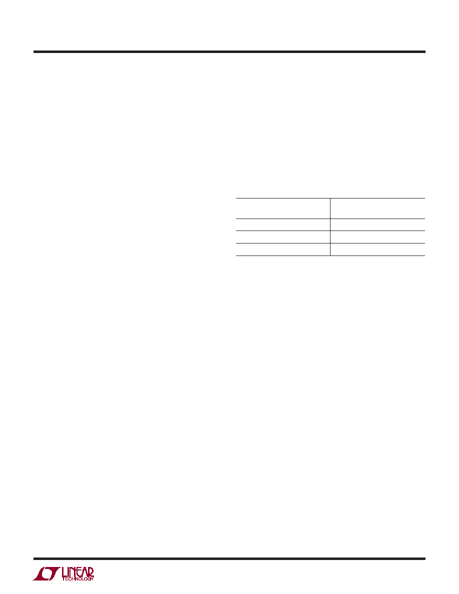
the 100:1 filter operation. This is shown in Table 1.
When Pin 12 is shorted to the negative supply pin, the filter
operation is stopped and the bandpass and lowpass
outputs act as a S/H circuit holding the last sample. The
hold step is 20mV and the droop rate is 150V/second!
Table 1
VOLTAGE RANGE OF PIN 12
TOTAL POWER SUPPLY
FOR 100:1 OPERATION
5V
2.5 ± 0.5V
10V
5V ± 1V
15V
7.5V ± 1.5V
S1A, S1B (Pins 5 and 16)
These are voltage signal input pins and, if used, they
should be driven with a source impedance below 5k. The
S1A, S1B pins can be used to alter the CLK to center
frequency ratio (fCLK/f0) of the filter (see Modes 1b, 1c, 2a,
2b) or to feedforward the input signal for allpass filter
configurations (see Modes 4 and 5). When these pins are
not used, they should be tied to the AGND pin.
SA/B (Pin 6)
When SA/B is high, the S2 input of the filter’s voltage
summer (see Block Diagram) is tied to the lowpass output.
This frees the S1 pin to realize various modes of operation
for improved applications flexibility. When the SA/B pin is
connected to the negative supply, the S2 input switches to
ground and internally becomes inactive. This improves
the filter noise performance and typically lowers the value
of the offset VOS2.
AGND (Pln 15)
This should be connected to the system ground for dual
supply operation. When the LTC1060 operates with a
single positive supply, the analog ground pin should be
tied to 1/2 supply and bypassed with a 0.1F capacitor, as
shown in the application, “Single 5V, Gain of 1000 4th
Order Bandpass Filter.” The positive inputs of all the
Power Supplies
The V +A and V +D (pins 7 and 8) and the V–A and V–D
(Pins 14 and 13) are, respectively, the analog and digital
positive and negative supply pins. For most cases, Pins 7
and 8 should be tied together and bypassed by a 0.1F disc
ceramic capacitor. The same holds for Pins 13 and 14. If
the LTC1060 operates in a high digital noise environment,
the supply pins can be bypassed separately. Pins 7 and 8
are internally connected through the IC substrate and
should be biased from the same DC source. Pins 13 and
14 should also be biased from the same DC source.
The LTC1060 is designed to operate with ±2.5V supply
(or single 5V) and with ± 5V to ±8V supplies. The mini-
mum supply, where the filter operates reliably, is ± 2.37V.
With low supply operation, the maximum input clock
frequency is about 500kHz. Beyond this, the device exhib-
its excessive Q enhancement and center frequency errors.
Clock Input Pins and Level Shift
The level shift (LSh) Pin 9 is used to accommodate T2L or
CMOS clock levels. With dual supplies equal or higher
to ±4.5V, Pin 9 should be connected to ground (same
potential as the AGND pin). Under these conditions the
clock levels can be T2L or CMOS. With single supply
operation, the negative supply pins and the LSh pin should
be tied to the system ground. The AGND, Pin 15, should
be biased at 1/2 supplies, as shown in the “Single 5V Gain
of 1000 4th Order Bandpass Filter” circuit. Again, under
these conditions, the clock levels can be T2L or CMOS. The
input clock pins (10,11) share the same level shift pin.
The clock logic threshold level over temperature is
typically 1.5V ± 0.1V above the LSh pin potential. The duty
cycle of the input clock should be close to 50%. For clock
frequencies below 1MHz, the (fCLK/f0) ratio is independent
from the clock input levels and from its rise and fall times.
Fast rising clock edges, however, improve the filter DC
offsets. For clock frequencies above 1MHz, T2L level
clocks are recommended.
50/100/Hold (Pin 12)
By tying Pin 12 to (V+A and V +D), the filter operates in the
50:1 mode. With ±5V supplies, Pin 12 can be typically 1V
below the positive supply without affecting the 50:1
PIN DESCRIPTION AND APPLICATIONS INFORMATIO
UU
U
W
相关PDF资料 |
PDF描述 |
|---|---|
| VE-27N-IY-F4 | CONVERTER MOD DC/DC 18.5V 50W |
| VE-27M-IY-F1 | CONVERTER MOD DC/DC 10V 50W |
| VE-27L-IY-F3 | CONVERTER MOD DC/DC 28V 50W |
| VE-27K-IY-F1 | CONVERTER MOD DC/DC 40V 50W |
| VE-27J-IY-F4 | CONVERTER MOD DC/DC 36V 50W |
相关代理商/技术参数 |
参数描述 |
|---|---|
| LTC1060CN#PBF | 功能描述:IC FILTER BUILDING BLOCK 20-DIP RoHS:是 类别:集成电路 (IC) >> 接口 - 滤波器 - 有源 系列:- 产品培训模块:Lead (SnPb) Finish for COTS Obsolescence Mitigation Program 标准包装:1,000 系列:- 滤波器类型:连续时间,带通低通 频率 - 截止或中心:150kHz 滤波器数:4 滤波器阶数:8th 电源电压:4.74 V ~ 11 V,±2.37 V ~ 5.5 V 安装类型:表面贴装 封装/外壳:28-SOIC(0.295",7.50mm 宽) 供应商设备封装:28-SOIC W 包装:带卷 (TR) |
| LTC1060CS | 制造商:LINER 制造商全称:Linear Technology 功能描述:Universal Dual Filter Building Block |
| LTC1060CSW | 功能描述:IC FILTER BUILDING BLOCK 20-SOIC RoHS:否 类别:集成电路 (IC) >> 接口 - 滤波器 - 有源 系列:- 产品培训模块:Lead (SnPb) Finish for COTS Obsolescence Mitigation Program 标准包装:1,000 系列:- 滤波器类型:连续时间,带通低通 频率 - 截止或中心:150kHz 滤波器数:4 滤波器阶数:8th 电源电压:4.74 V ~ 11 V,±2.37 V ~ 5.5 V 安装类型:表面贴装 封装/外壳:28-SOIC(0.295",7.50mm 宽) 供应商设备封装:28-SOIC W 包装:带卷 (TR) |
| LTC1060CSW#PBF | 功能描述:IC FILTER BUILDING BLOCK 20-SOIC RoHS:是 类别:集成电路 (IC) >> 接口 - 滤波器 - 有源 系列:- 产品培训模块:Lead (SnPb) Finish for COTS Obsolescence Mitigation Program 标准包装:1,000 系列:- 滤波器类型:连续时间,带通低通 频率 - 截止或中心:150kHz 滤波器数:4 滤波器阶数:8th 电源电压:4.74 V ~ 11 V,±2.37 V ~ 5.5 V 安装类型:表面贴装 封装/外壳:28-SOIC(0.295",7.50mm 宽) 供应商设备封装:28-SOIC W 包装:带卷 (TR) |
| LTC1060CSW#PBF | 制造商:Linear Technology 功能描述:IC SW CAP FILTER UNIVERSAL 20KHZ SOIC-20 |
发布紧急采购,3分钟左右您将得到回复。