- 您现在的位置:买卖IC网 > PDF目录11022 > LTC1061CSW#PBF (Linear Technology)IC FILTR BUILDNG BLK TRPL 20SOIC PDF资料下载
参数资料
| 型号: | LTC1061CSW#PBF |
| 厂商: | Linear Technology |
| 文件页数: | 2/16页 |
| 文件大小: | 0K |
| 描述: | IC FILTR BUILDNG BLK TRPL 20SOIC |
| 标准包装: | 38 |
| 滤波器类型: | 通用开关电容器 |
| 频率 - 截止或中心: | 35kHz |
| 滤波器数: | 3 |
| 滤波器阶数: | 6th |
| 电源电压: | 4.74 V ~ 16 V,±2.37 V ~ 8 V |
| 安装类型: | 表面贴装 |
| 封装/外壳: | 20-SOIC(0.295",7.50mm 宽) |
| 供应商设备封装: | 20-SOIC |
| 包装: | 管件 |
LTC1061
10
1061fe
fIN (kHz)
1.0
V
OUT
/V
IN
(dB)
–10
3.0
1061 F14
–30
–60
–80
1.5
2.0
2.5
3.5
–50
–40
–20
0
–70
–90
VS = ±5V
fCLK = 130kHz
R11 = 576k
R31 = 562k
Rh11 = 28.7k
R22 = 10.7k
R42 = 10k
Rl2 = 10k
R33 = 75k
R21 = 10k
R41 = 10.7k
Rl11 = 40.2k
R32 = 562k
Rh2 = 14k
R23 = 2.94k
NOTE: FOR CLOCK FREQUENCIES
ABOVE 500kHz, CONNECT A 5pF
IN PARALLEL WITH R41 AND R42.
STANDARD 1%
RESISTOR VALUES
fIN (kHz)
1.0
V
OUT
/V
IN
(dB)
–10
3.0
1061 F13
–30
–60
–70
1.5
2.0
2.5
3.5
–50
–40
–20
0
BW1
BW2
2.6kHz
STANDARD 1%
RESISTOR VALUES
R11 = 165k
R31 = 143k
Rh1 = 10k
R22 = 20k
R42 = 15.4k
Rl2 = 10k
R33 = 169k
R21 = 10k
R41 = 13k
Rl1 = 10.5k
R32 = 221k
Rh2 = 10.5k
R23 = 84.5k
NOTES: USE A 15pF CAPACITOR
BETWEEN PINS 17 AND 18.
PIN 7 IS GROUNDED.
VS = ±5V
fCLK = 260kHz
20
19
18
17
16
15
14
13
12
11
1
2
3
4
5
6
7
8
9
10
R32
VIN
1061 F12
LTC1061
R22
Rh2
R31
R41
R33
R23
T2L, CMOS
CLOCK INPUT
V –
R42
V +
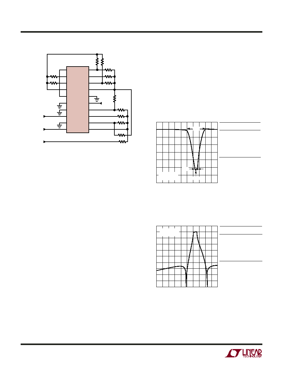
NOTES: FOR NOTCH RESPONSES, PIN 7 SHOULD BE
PREFERABLY CONNECTED TO GROUND AND THE
FILTER OUTPUT IS PIN 3.
FOR BANDPASS OR LOWPASS RESPONSES, PIN 7
CAN BE EITHER AT GROUND OR POSITIVE SUPPLY,
AND THE FILTER OUTPUT IS PIN 2 OR PIN 1.
Rl2
Rl1
R21
R11
Rh1
ODES OF OPERATIO
W
U
center frequencies, Qs, and notch frequencies are (fO1 =
0.969, Q1 = 54.3, fn1 = 0.84, fO2 = 1.031, Q2 = 54.3, fn2 =
1.187, fO3 = 1, Q3 = 26.2). The output of the filter is the BP
output of Side A, Pin 2.
Lowpass filters with stopband notches can also be realized
by using Figure 12 provided that 6th order lowpass filter
approximations with 2 stopband notches can be synthe-
sized. Literature describing elliptic double terminated (RLC)
Figure 14. Resistor Values and Amplitude Response of Figure 12
Topology. The Bandpass Filter is Centered Around 2600Hz when
Operating with a 130kHz Clock.
Figure 13. Resistor Values and Amplitude Response of
Figure 12 Topology. The Notch is Centered at 2600Hz.
Figure 12. 6th Order Elliptic Bandpass, Lowpass
or Notch Topology
Figure 13 shows the measured frequency response of the
circuit Figure 12 configured to provide a notch function.
The filter output is taken out of pin 3. The resistor values
are standard 1%.
The ratio of the 0dB width, BW1, to the notch width BW2,
is 5:1 and matches the theoretical design value. The
measured notch depth was –53dB versus –56dB theoreti-
cal and the clock-to-center notch frequency ratio is 100:1.
Figure 14 shows the measured frequency response of the
circuit topology, Figure 12, but with pole/zero locations
configured to provide a high Q, 6th order elliptic bandpass
filter operating with a clock-to-center frequency ratio of
50:1 or 100:1. The theoretical passband ripple, stopband
attenuation and stopband to ripple bandwidth ratio are
0.5dB, 56dB, 5:1 respectively. The obtained results with
1% standard resistor values closely match the theoretical
frequency response. For this application, the normalized
相关PDF资料 |
PDF描述 |
|---|---|
| LTC1164-6CN | IC FILTR 8TH ORDER LOWPASS 14DIP |
| LTC1562ACG#TR | IC FILTER UNIV RC QUAD LN 20SSOP |
| LTC1562ACG#PBF | IC FILTER UNIV RC QUAD LN 20SSOP |
| LTC1562ACG | IC FILTER UNIVRSL RC QUAD 20SSOP |
| LTC1562ACG#TRPBF | IC FILTER UNIV RC QUAD LN 20SSOP |
相关代理商/技术参数 |
参数描述 |
|---|---|
| LTC1061M | 制造商:LINER 制造商全称:Linear Technology 功能描述:High Performance Triple Universal Filter Building Block |
| LTC1061MJ | 制造商:LINER 制造商全称:Linear Technology 功能描述:High Performance Triple Universal Filter Building Block |
| LTC1061MJ/883 | 制造商:Linear Technology 功能描述:Active Filter Triple SW-CAP UNIV 6th Order 35kHz 20-Pin CDIP |
| LTC1061MJ/883B | 制造商:未知厂家 制造商全称:未知厂家 功能描述:Analog Filter |
| LTC1061S | 制造商:LINER 制造商全称:Linear Technology 功能描述:High Performance Triple Universal Filter Building Block |
发布紧急采购,3分钟左右您将得到回复。