- 您现在的位置:买卖IC网 > PDF目录11022 > LTC1061CSW#TR (Linear Technology)IC BUILDING BLK TRPL FLTR 20SOIC PDF资料下载
参数资料
| 型号: | LTC1061CSW#TR |
| 厂商: | Linear Technology |
| 文件页数: | 12/16页 |
| 文件大小: | 0K |
| 描述: | IC BUILDING BLK TRPL FLTR 20SOIC |
| 标准包装: | 1,000 |
| 滤波器类型: | 通用开关电容器 |
| 频率 - 截止或中心: | 35kHz |
| 滤波器数: | 3 |
| 滤波器阶数: | 6th |
| 电源电压: | 4.74 V ~ 16 V,±2.37 V ~ 8 V |
| 安装类型: | 表面贴装 |
| 封装/外壳: | 20-SOIC(0.295",7.50mm 宽) |
| 供应商设备封装: | 20-SOIC |
| 包装: | 带卷 (TR) |
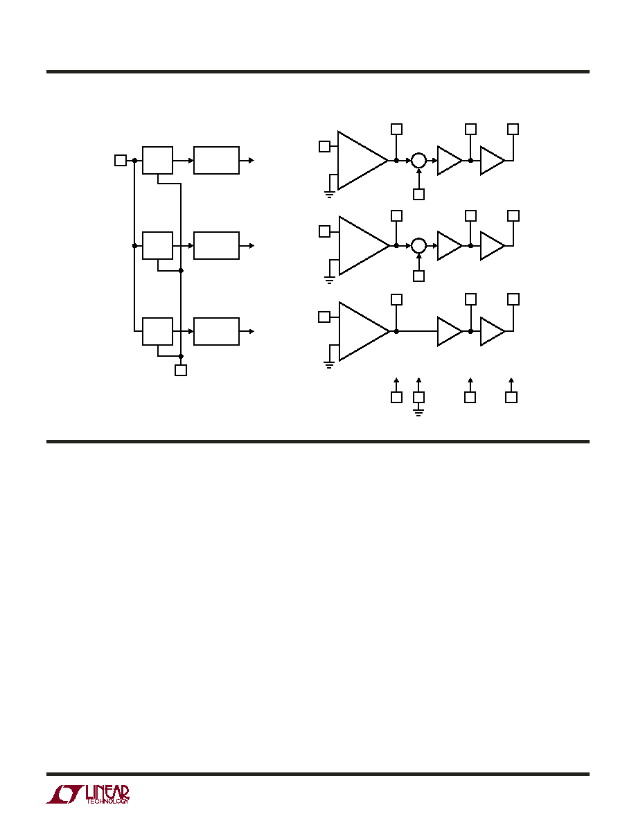
5
LTC1061
1061fe
DESCRIPTIO A D
U
PI
U
APPLICATIO
U
HI TS
U
–
+
Σ
+
∫
Σ
LEVEL
SHIFT
LEVEL
SHIFT
LEVEL
SHIFT
CLOCK
GENERATOR
CLOCK
GENERATOR
CLOCK
GENERATOR
CLK
(8)
LEVEL SHIFT
(9)
TO FILTER A
TO FILTER B
TO FILTER C
+
∫
+
∫
+
∫
+
∫
+
∫
50/100/
HOLD
(7)
AGND
(6)
V+
(10)
V –
(15)
HPC
(12)
S1B
(16)
BPC
(13)
LPC
(14)
S1A
(5)
NB
(18)
BPB
(19)
LPB
(20)
NA
(3)
BPA
(2)
LPA
(1)
INVA
(4)
INVB
(17)
INVC
(11)
1061 BD
+
–
+
–
+
–
+
frequencies below 500kHz the clock “on” time can be as
low as 300ns. The maximum clock frequency for
±5V
supplies and above is 2.4MHz.
S1A, S1B (Pins 5, 16)
These are voltage input pins. If used, they should be driven
with a source impedance below 5k
. when they are not
used, they should be tied to the analog ground Pin 6.
AGND (Pin 6)
When the LTC1061 operates with dual supplies, Pin 6
should be tied to system ground. When the LTC1061
operates with a single positive supply, the analog ground
pin should be tied to 1/2 supply, Figure 1. The positive
input of all the internal op amps, as well as the common
reference of all the internal switches, are internally tied to
the analog ground pin. Because of this, a “clean” ground
is recommended.
Power Supplies (Pins 10, 15)
They should be bypassed with 0.1
F disc ceramic. Low
noise, nonswitching, power supplies are recommended.
The device operates with a single 5V supply, Figure 1, and
with dual supplies. The absolute maximum operating
power supply voltage is
±9V.
Clock and Level shift (Pins 8, 9)
When the LTC1061 operates with symmetrical dual sup-
plies the level shift Pin 9 should be tied to analog ground.
For single 5V supply operation, the level shift pin should be
tied to Pin 15 which will be the system ground. The typical
logic threshold levels of the clock pin are as follows: 1.65V
above the level shift pin for
±5V supply operation, 1.75V
for
±7.5V and above, and 1.4V for single 5V supply
operation. The logic threshold levels vary
±100mV over
the full military temperature range. The recommended
duty cycle of the input clock is 50% although for clock
BLOCK DIAGRA
W
相关PDF资料 |
PDF描述 |
|---|---|
| LTC1061CSW#PBF | IC FILTR BUILDNG BLK TRPL 20SOIC |
| LTC1164-6CN | IC FILTR 8TH ORDER LOWPASS 14DIP |
| LTC1562ACG#TR | IC FILTER UNIV RC QUAD LN 20SSOP |
| LTC1562ACG#PBF | IC FILTER UNIV RC QUAD LN 20SSOP |
| LTC1562ACG | IC FILTER UNIVRSL RC QUAD 20SSOP |
相关代理商/技术参数 |
参数描述 |
|---|---|
| LTC1061M | 制造商:LINER 制造商全称:Linear Technology 功能描述:High Performance Triple Universal Filter Building Block |
| LTC1061MJ | 制造商:LINER 制造商全称:Linear Technology 功能描述:High Performance Triple Universal Filter Building Block |
| LTC1061MJ/883 | 制造商:Linear Technology 功能描述:Active Filter Triple SW-CAP UNIV 6th Order 35kHz 20-Pin CDIP |
| LTC1061MJ/883B | 制造商:未知厂家 制造商全称:未知厂家 功能描述:Analog Filter |
| LTC1061S | 制造商:LINER 制造商全称:Linear Technology 功能描述:High Performance Triple Universal Filter Building Block |
发布紧急采购,3分钟左右您将得到回复。