- 您现在的位置:买卖IC网 > PDF目录11022 > LTC1061CSW#TRPBF (Linear Technology)IC FILTR BUILDNG BLK TRPL 20SOIC PDF资料下载
参数资料
| 型号: | LTC1061CSW#TRPBF |
| 厂商: | Linear Technology |
| 文件页数: | 5/16页 |
| 文件大小: | 0K |
| 描述: | IC FILTR BUILDNG BLK TRPL 20SOIC |
| 标准包装: | 1,000 |
| 滤波器类型: | 通用开关电容器 |
| 频率 - 截止或中心: | 35kHz |
| 滤波器数: | 3 |
| 滤波器阶数: | 6th |
| 电源电压: | 4.74 V ~ 16 V,±2.37 V ~ 8 V |
| 安装类型: | 表面贴装 |
| 封装/外壳: | 20-SOIC(0.295",7.50mm 宽) |
| 供应商设备封装: | 20-SOIC |
| 包装: | 带卷 (TR) |
13
LTC1061
1061fe
fIN (kHz)
1
V
OUT
/V
IN
(dB)
–10
9
1061 F22
–30
–60
–80
3
5
7
0
–50
–40
–20
0
–70
–90
2
4
68
10
STANDARD 1%
RESISTOR VALUES
R11 = 54.9k
R31 = 34.8k
Rh1 = 28.7k
R22 = 68.1k
R42 = 10k
Rl2 = 16.2k
R33 = 75k
R21 = 24.3k
R41 = 10k
Rl1 = 280k
R32 = 18.2k
Rh2 = 10.2k
R23 = 10k
R43 = 14k
NOTE: FOR CLOCK FREQUEN-
CIES ABOVE 300kHz, ADD
A CAPACITOR C ACROSS
R21 AND R22 SUCH AS
(1/2
πR21C) = fCLK
20
19
18
17
16
15
14
13
12
11
1
2
3
4
5
6
7
8
9
10
VIN
1061 F21
LTC1061
Rh2
R43
R33
T2L, CMOS
CLOCK INPUT
V –
V +
Rl2
R32
R22
R42
R31
R41
Rl1
R21
R11
Rh1
R23
VOUT
ODES OF OPERATIO
W
U
higher frequency notch provided by the side A of the
LTC1061. As shown in Figure 22, the highpass corner
frequency is 3.93kHz and the higher notch frequency is
3kHz while the filter operates with a 300kHz clock. The
center frequencies, Qs, and notches of Figure 22, when
normalized to the highpass cutoff frequency, are (fO1 =
1.17, Q1 = 2.24, fn1 = 0.242, fO2 = 1.96, Q2 = 0.7, fn2 = 0.6,
fO3 = 0.987, fn3 = 0.753, Q3 = 10). When compared with the
topology of Figure 16, this approach uses lower and more
restricted clock frequencies. The obtained notch in Mode
2 is shallower although the topology is more efficient.
Output Noise
The wideband RMS noise of the LTC1061 outputs is nearly
independent from the clock frequency. The LTC1061
noise when operating with
±2.5V supply is lower, as Table
3 indicates. The noise at the bandpass and lowpass
outputs increases rough as the
√Q. Also the noise in-
creases when the clock-to-center frequency ratio is al-
tered with external resistors to exceed the internally set
100:1 or 50:1 ratios. Under this condition, the noise
increases square root-wise.
Output Offsets
The equivalent input offsets of the LTC1061 are shown in
Figure 23. The DC offset at the filter bandpass output is
always equal to VOS3. The DC offsets at the remaining two
outputs (Notch and LP) depend on the mode of operation
and external resistor ratios. Table 4 illustrates this.
It is important to know the value of the DC output offsets,
especially when the filter handles input signals with large
dynamic range. As a rule of thumb, the output DC offsets
increase when:
1. The Qs decrease
2. The ratio (fCLK/fO) increases beyond 100:1. This is
done by decreasing either the (R2/R4) or the R6/(R5
+ R6) resistor ratios.
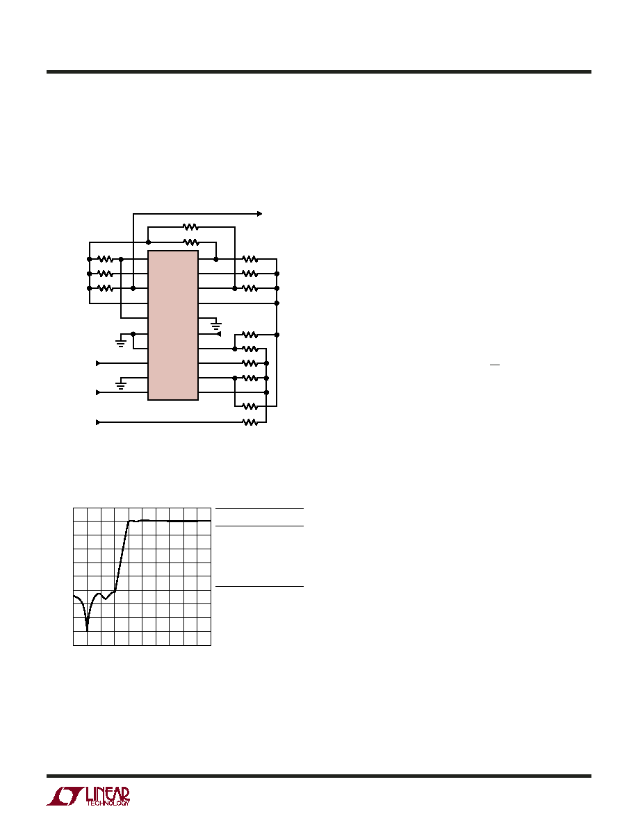
Figure 21 shows the side A of the LTC1061 connected in
Mode 2 while sides B and C are in Mode 3a. This topology
can be used to synthesize elliptic bandpass, highpass and
notch filters. The elliptic highpass of Figure 17 is synthe-
sized again, Figure 22, but the clock is now locked onto the
Figure 22. 6th Order Elliptic Highpass Filter Operating with a
Clock-to-Cutoff Frequency Ratio of 75:1 and Using the Topology
of Figure 21
Figure 21. LTC1061 with Side A is Connected in Mode 2 While
Side B, C are in Mode 3a. Topology is Useful for Elliptic
Highpass, Notch and Bandpass Filters.
相关PDF资料 |
PDF描述 |
|---|---|
| LTC1061CSW#TR | IC BUILDING BLK TRPL FLTR 20SOIC |
| LTC1061CSW#PBF | IC FILTR BUILDNG BLK TRPL 20SOIC |
| LTC1164-6CN | IC FILTR 8TH ORDER LOWPASS 14DIP |
| LTC1562ACG#TR | IC FILTER UNIV RC QUAD LN 20SSOP |
| LTC1562ACG#PBF | IC FILTER UNIV RC QUAD LN 20SSOP |
相关代理商/技术参数 |
参数描述 |
|---|---|
| LTC1061M | 制造商:LINER 制造商全称:Linear Technology 功能描述:High Performance Triple Universal Filter Building Block |
| LTC1061MJ | 制造商:LINER 制造商全称:Linear Technology 功能描述:High Performance Triple Universal Filter Building Block |
| LTC1061MJ/883 | 制造商:Linear Technology 功能描述:Active Filter Triple SW-CAP UNIV 6th Order 35kHz 20-Pin CDIP |
| LTC1061MJ/883B | 制造商:未知厂家 制造商全称:未知厂家 功能描述:Analog Filter |
| LTC1061S | 制造商:LINER 制造商全称:Linear Technology 功能描述:High Performance Triple Universal Filter Building Block |
发布紧急采购,3分钟左右您将得到回复。