- 您现在的位置:买卖IC网 > PDF目录11035 > LTC1064CSW#PBF (Linear Technology)IC FILTR BUILDNG BLK QUAD 24SOIC PDF资料下载
参数资料
| 型号: | LTC1064CSW#PBF |
| 厂商: | Linear Technology |
| 文件页数: | 17/20页 |
| 文件大小: | 0K |
| 描述: | IC FILTR BUILDNG BLK QUAD 24SOIC |
| 标准包装: | 32 |
| 滤波器类型: | 通用开关电容器 |
| 频率 - 截止或中心: | 140kHz |
| 滤波器数: | 4 |
| 滤波器阶数: | 8th |
| 电源电压: | ±2.37 V ~ 8 V |
| 安装类型: | 表面贴装 |
| 封装/外壳: | 24-SOIC(0.295",7.50mm 宽) |
| 供应商设备封装: | 24-SOIC |
| 包装: | 管件 |
| 产品目录页面: | 1324 (CN2011-ZH PDF) |
LTC1064
6
1064fb
24
23
22
21
20
19
18
17
16
15
14
13
1
2
3
4
5
6
7
8
9
10
11
12
V–
CLK
50/100
AGND
V+
ANALOG
GROUND
PLANE
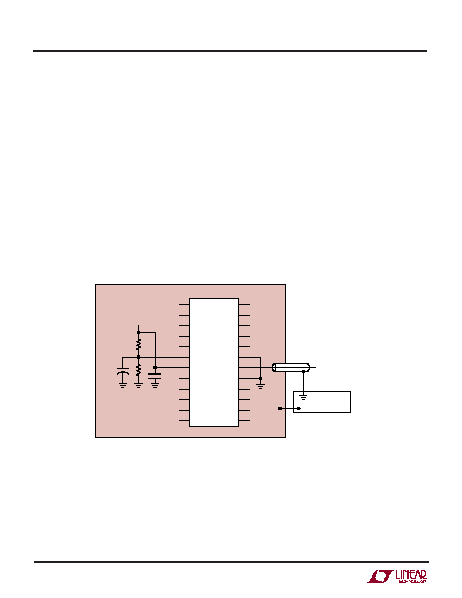
NOTE: PINS 5, 8, 20, IF NOT USED, SHOULD BE CONNECTED TO PIN 6
CLOCK INPUT
V+ = 15V, TRIP VOLTAGE = 7V
V+ = 10V, TRIP VOLTAGE = 6.4V
V+ = 5V, TRIP VOLTAGE = 3V
TO DIGITAL
GROUND
V+
LTC1064
0.1
F
5k
1064 F01
5k
1
F
V+/2
+
PIN FUNCTIONS
UU
U
AGND (Pin 6): Analog Ground. When the LTC1064 oper-
ates with dual supplies, Pin 6 should be tied to system
ground. When the LTC1064 operates with a single positive
supply, the analog ground pin should be tied to 1/2 supply
and it should be bypassed with a 1
F solid tantalum in
parallel with a 0.1
F ceramic capacitor, Figure 1. The
positive input of all the internal op amps, as well as the
common reference of all the internal switches, are inter-
nally tied to the analog ground pin. Because of this, a very
“clean” ground is recommended.
50/100 (Pin 17): By tying Pin 17 to V +, all filter sections
operate with a clock-to-center frequency ratio internally
set at 50:1. When Pin 17 is at mid-supplies, sections B and
C operate with (fCLK/fO) = 50:1 and sections A and D
operate at 100:1. When Pin 17 is shorted to the negative
supply pin, all filter sections operate with (fCLK/fO) =
100:1.
V +, V – (Pins 7, 19): Power Supplies. They should be
bypassed with a 0.1
F ceramic capacitor. Low noise,
nonswitching power supplies are recommended. The de-
vice operates with a single 5V supply and with dual
supplies. The absolute maximum operating power supply
voltage is
±8V.
CLK (Pin 18): Clock. For
±5V supplies the logic threshold
level is 1.4V. For
±8V and 0V to 5V supplies the logic
threshold levels are 2.2V and 3V respectively. The logic
threshold levels vary
±100mV over the full military tem-
perature range. The recommended duty cycle of the input
clock is 50%, although for clock frequencies below 500kHz,
the clock “on” time can be as low as 200ns. The maximum
clock frequency for
±5V supplies is 4MHz. For ±7V
supplies and above, the maximum clock frequency is
7MHz.
Figure 1. Single Supply Operation
相关PDF资料 |
PDF描述 |
|---|---|
| VE-JWD-IW-B1 | CONVERTER MOD DC/DC 85V 100W |
| QPI-12LZ | FILTER VI CHIP 48V 7A LGA |
| VE-JWB-IW-B1 | CONVERTER MOD DC/DC 95V 100W |
| LTC1060ACN#PBF | IC FILTER BUILDING BLOCK 20-DIP |
| VE-JW4-IW-B1 | CONVERTER MOD DC/DC 48V 100W |
相关代理商/技术参数 |
参数描述 |
|---|---|
| LTC1064M | 制造商:LINER 制造商全称:Linear Technology 功能描述:Low Noise, Fast, Quad Universal Filter Building Block |
| LTC1064MJ | 制造商:LINER 制造商全称:Linear Technology 功能描述:Low Noise, Fast, Quad Universal Filter Building Block |
| LTC1065 | 制造商:LINER 制造商全称:Linear Technology 功能描述:DC Accurate, Clock-Tunable Linear Phase 5th Order Bessel Lowpass Filter |
| LTC1065_09 | 制造商:LINER 制造商全称:Linear Technology 功能描述:DC Accurate, Clock-Tunable Linear Phase 5th Order Bessel Lowpass Filter |
| LTC1065C | 制造商:LINER 制造商全称:Linear Technology 功能描述:DC Accurate, Clock-Tunable Linear Phase 5th Order Bessel Lowpass Filter |
发布紧急采购,3分钟左右您将得到回复。