- 您现在的位置:买卖IC网 > PDF目录11026 > LTC1065ISW#TR (Linear Technology)IC FILTER LP 5TH ORD LIN 16SOIC PDF资料下载
参数资料
| 型号: | LTC1065ISW#TR |
| 厂商: | Linear Technology |
| 文件页数: | 14/16页 |
| 文件大小: | 0K |
| 描述: | IC FILTER LP 5TH ORD LIN 16SOIC |
| 标准包装: | 1,000 |
| 滤波器类型: | 贝塞尔,低通开关电容器 |
| 频率 - 截止或中心: | 50kHz |
| 滤波器数: | 1 |
| 滤波器阶数: | 5th |
| 电源电压: | ±2.37 V ~ 8 V |
| 安装类型: | 表面贴装 |
| 封装/外壳: | 16-SOIC(0.295",7.50mm 宽) |
| 供应商设备封装: | 16-SOIC |
| 包装: | 带卷 (TR) |
7
LTC1065
1065fb
CLOCK FREQUENCY (MHz)
1
MAXIMUM
LOAD
CAPACITANCE
(pF
)
200
180
160
140
120
100
80
60
40
20
0
310
1065 F02
24
5
6 78 9
VS = ±2.5V
VS = ±5V
VS = ±7.5V
TA = 25°C
PI FU CTIO S
U
UU
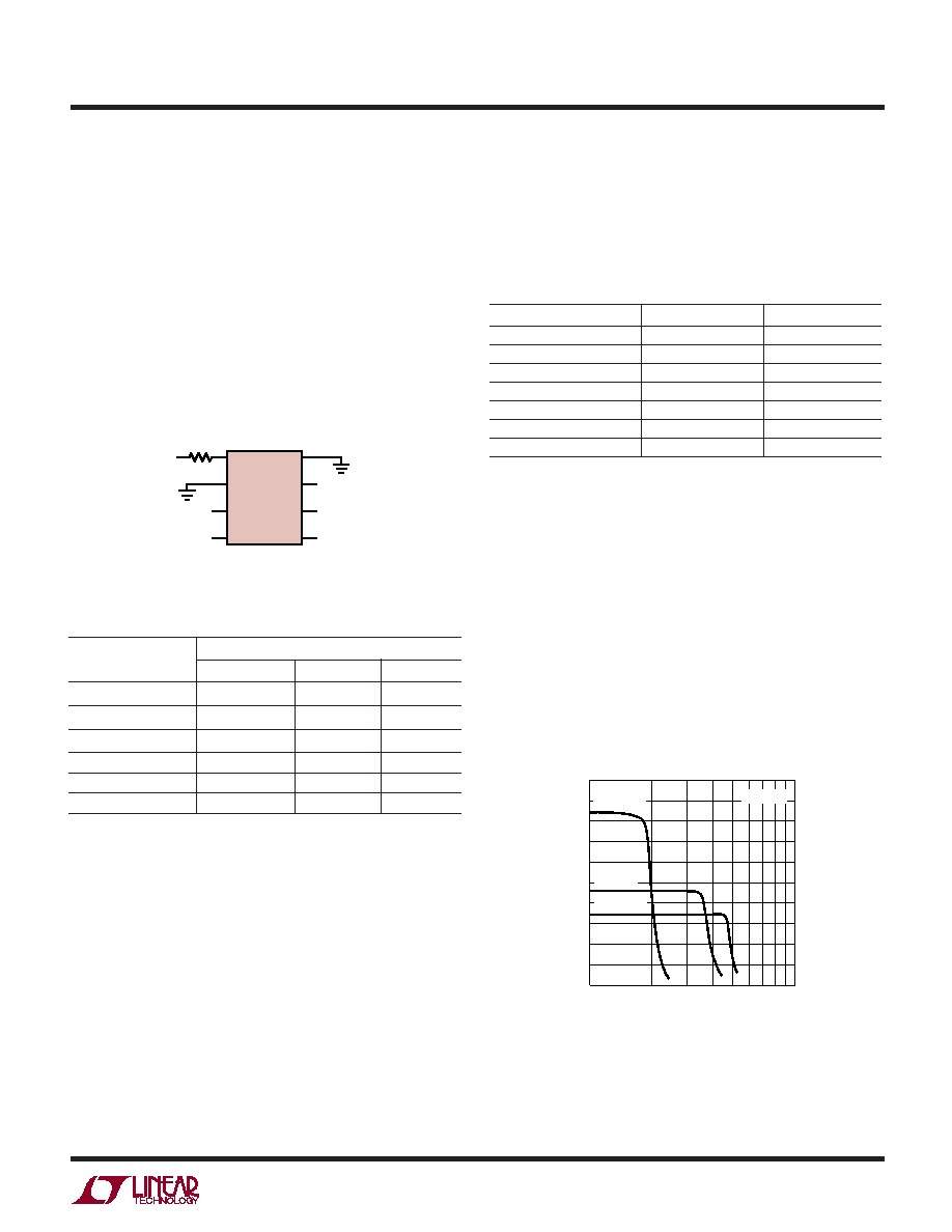
Input Pin (Pin 1, N Package)
Pin 1 is the filter input and it is connected to an internal
switched-capacitor resistor. If the input pin is left floating,
the filter output will saturate. The DC input impedance of
pin 1 is very high; with
±5V supplies and 1MHz clock, the
DC input impedance is typically 1G
. A resistor RIN in
series with the input pin will not alter the value of the filter’s
DC output offset (Figure 1). RIN should however, be limited
to a maximum value (Table 1), otherwise the filter’s pass-
band will be affected. Refer to the Applications Information
section for more details.
VIN
VOUT
1065 F01
V–
V+
RIN 1
2
3
4
8
7
6
5
LTC1065
fCLK
Figure 1.
Table 1. RIN(MAX) vs Clock and Power Supply
RIN(MAX)
VS = ±7.5V
VS = ±5V
VS = ±2.5V
fCLK = 4MHz
1.82k
–
fCLK = 3MHz
3.01k
2.49k
–
fCLK = 2MHz
4.32k
3.65k
2.37k
fCLK = 1MHz
9.09k
8.25k
7.5k
fCLK = 500kHz
17.8k
16.9k
fCLK = 100kHz
95.3k
90.9k
100:1. The high (VHIGH) and low (VLOW) clock logic
threshold levels are illustrated in Table 2. Square wave
clocks with duty cycles between 30% and 50% are strongly
recommended. Sinewave clocks are not recommended.
Output Pin (Pin 7, N Package)
Pin 7 is the filter output. This pin can typically source over
20mA and sink 2mA. Pin 7 should not drive long coax
cables, otherwise the filter’s total harmonic distortion will
degrade. The maximum load the filter output can drive and
still maintain the distortion levels, shown in the Typical
Performance Characteristics, is 20k.
Clock Input Pin (Pin 5, N Package)
An external clock, when applied to pin 5, tunes the filter
cutoff frequency. The clock-to-cutoff frequency ratio is
Table 2. Clock Pin Threshold Levels
POWER SUPPLY
VHIGH
VLOW
VS = ±2.5V
1.5V
0.5V
VS = ±5V
3V
1V
VS = ±7.5V
4.5V
1.5V
VS = ±8V
4.8V
1.6V
VS = 5V, 0V
4V
3V
VS = 12V, 0V
9.6V
7.2V
VS =15V, 0V
12V
9V
Clock Output Pin (Pin 4, N Package)
Any external clock applied to the clock input pin appears
at the clock output pin. The duty cycle of the clock output
equals the duty cycle of the external clock applied to the
clock input pin. The clock output pin swings to the power
supply rails. When the LTC1065 is used in a self-clocking
mode, the clock of the internal oscillator appears at the
clock output pin with a 30% duty cycle. The clock output
pin can be used to drive other LTC1065s or other ICs. The
maximum capacitance, CL(MAX), the clock output pin can
drive is illustrated in Figure 2.
Figure 2. Maximum Load Capacitance at the Clock Output Pin
相关PDF资料 |
PDF描述 |
|---|---|
| VE-B0M-IY-F4 | CONVERTER MOD DC/DC 10V 50W |
| VE-B0M-IY-F1 | CONVERTER MOD DC/DC 10V 50W |
| LTC1065ISW#PBF | IC FILTR 5TH ORDR LOWPASS 16SOIC |
| VE-B0L-IY-F1 | CONVERTER MOD DC/DC 28V 50W |
| LTC1065ISW | IC FILTR 5TH ORDR LOWPASS 16SOIC |
相关代理商/技术参数 |
参数描述 |
|---|---|
| LTC1065M | 制造商:LINER 制造商全称:Linear Technology 功能描述:DC Accurate, Clock-Tunable Linear Phase 5th Order Bessel Lowpass Filter |
| LTC1065MJ8 | 制造商:LINER 制造商全称:Linear Technology 功能描述:DC Accurate, Clock-Tunable Linear Phase 5th Order Bessel Lowpass Filter |
| LTC1066-1 | 制造商:LINER 制造商全称:Linear Technology 功能描述:14-Bit DC Accurate Clock-Tunable, 8th Order Elliptic or Linear Phase Lowpass Filter |
| LTC1066-1_09 | 制造商:LINER 制造商全称:Linear Technology 功能描述:14-Bit DC Accurate Clock-Tunable, 8th Order Elliptic or Linear Phase Lowpass Filter |
| LTC1066-1CS | 制造商:LINER 制造商全称:Linear Technology 功能描述:14-Bit DC Accurate Clock-Tunable, 8th Order Elliptic or Linear Phase Lowpass Filter |
发布紧急采购,3分钟左右您将得到回复。