- 您现在的位置:买卖IC网 > PDF目录11021 > LTC1066-1CSW (Linear Technology)IC FILTR 8TH ORDR LOWPASS 18SOIC PDF资料下载
参数资料
| 型号: | LTC1066-1CSW |
| 厂商: | Linear Technology |
| 文件页数: | 18/20页 |
| 文件大小: | 0K |
| 描述: | IC FILTR 8TH ORDR LOWPASS 18SOIC |
| 标准包装: | 40 |
| 滤波器类型: | 贝塞尔,低通开关电容器 |
| 频率 - 截止或中心: | 50kHz |
| 滤波器数: | 1 |
| 滤波器阶数: | 8th |
| 电源电压: | 4.75 V ~ 16 V,±2.375 V ~ 8 V |
| 安装类型: | 表面贴装 |
| 封装/外壳: | 18-SOIC(0.295",7.50mm 宽) |
| 供应商设备封装: | 18-SOIC |
| 包装: | 管件 |
| 其它名称: | LTC1066-1CS |
LTC1066-1
7
10661fa
level threshold values for a dual or single supply operation.
Sine waves are not recommended for clock input frequen-
cies less than 100kHz, since excessively slow clock rise or
fall times generate internal clock jitter (maximum clock
rise or fall time
≤ 1s). The clock signal should be routed
from the left side of the IC package and perpendicular to it
to avoid coupling to any input or output analog signal path.
A 200
resistor between clock source and pin 9 will slow
down the rise and fall times of the clock to further reduce
charge coupling.
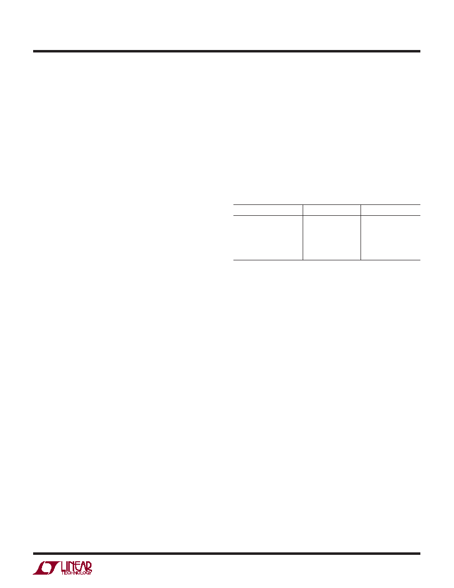
Table 5. Clock Source High and Low Threshold Levels
POWER SUPPLY
HIGH LEVEL
LOW LEVEL
Dual Supply =
±7.5V
≥ 2.18V
≤ 0.5V
Dual Supply =
±5V
≥ 1.45V
≤ 0.5V
Dual Supply =
±2.5V
≥ 0.73V
≤ –2.0V
Single Supply = 12V
≥ 7.80V
≤ 6.5V
Single Supply = 5V
≥ 1.45V
≤ 0.5V
50:1/100:1 Pin (8)
The DC level at pin 8 determines the ratio of the clock to
the filter cutoff frequency. When pin 8 is connected to
V + the clock-to-cutoff frequency ratio (fCLK/fCUTOFF) is
50:1 and the filter response is elliptic. The design of the
internal switched-capacitor filter was optimized for a 50:1
operation.
When pin 8 is connected to ground (or 1/2 supply for
single supply operation), the fCLK/fCUTOFF ratio is equal to
100:1 and the filter response is pseudolinear phase (see
Group Delay vs Frequency in Typical Performance Charac-
teristic section).
When pin 8 is connected to V – (or ground for single supply
operation), the fCLK/fCUTOFF ratio is 100:1 and the filter
response is transitional Butterworth elliptic. The Typical
Performance Characteristics provide all the necessary
information.
If the DC level at pin 8 is mechanically switched, a 10k
resistor should be connected between pin 8 and the DC
source.
Input Pins (2, 3, 14, 16)
Pin 3 (+IN A) and pin 2 (–IN A) are the positive and
negative inputs of an internal high performance op amp A
PIN FUNCTIONS
UU
U
Power Supply Pins (5, 18, 4, 10)
The power supply pins should be bypassed with a 0.1
F
capacitor to an adequate analog ground. The bypass
capacitors should be connected as close as possible to the
power supply pins. The V+ pins (5, 18) and the V – pins (4,
10) should always be tied to the same positive supply and
negative supply value respectively. Low noise linear sup-
plies are recommended. Switching power supplies are not
recommended as they will lower the filter dynamic range.
When the LTC1066-1 is powered up with dual supplies
and, if V+ is applied prior to a floating V –, connect a signal
diode (1N4148) between pin 10 and ground to prevent
power supply reversal and latch-up. A signal diode
(1N4148) is also recommended between pin 5 and ground
if the negative supply is applied prior to the positive supply
and the positive supply is floating. Note, in most labora-
tory supplies, reversed biased diodes are always con-
nected between the supply output terminals and ground,
and the above precautions are not necessary. However,
when the filter is powered up with conventional 3-terminal
regulators, the diodes are recommended.
Analog Ground Pin (15)
The filter performance depends on the quality of the
analog signal ground. For either dual or single supply
operation, an analog ground plane surrounding the pack-
age is recommended. The analog ground plane should be
connected to any digital ground at a single point. For dual
supply operation, pin 15 should be connected to the
analog ground plane. For single supply operation pin 15
should be biased at 1/2 supply and should be bypassed to
the analog ground plane with at least a 1
F capacitor (see
Typical Applications). For single 5V operation and for
fCLK ≥ 1.4MHz, pin 15 should be biased at 2V. This
minimizes passband gain and phase variations.
Clock Input Pin (9)
Any TTL or CMOS clock source with a square-wave output
and 50% duty cycle (
±10%) is an adequate clock source
for the device. The power supply for the clock source
should not be the filter’s power supply. The analog ground
for the filter should be connected to clock’s ground at a
single point only. Table 5 shows the clock’s low and high
相关PDF资料 |
PDF描述 |
|---|---|
| VE-20J-IY-F3 | CONVERTER MOD DC/DC 36V 50W |
| VE-20J-IY-F2 | CONVERTER MOD DC/DC 36V 50W |
| VE-20F-IY-F1 | CONVERTER MOD DC/DC 72V 50W |
| VE-20J-IY-F1 | CONVERTER MOD DC/DC 36V 50W |
| MC9S08SE8MWL | MCU 8BIT 8K FLASH 5V 28-SOIC |
相关代理商/技术参数 |
参数描述 |
|---|---|
| LTC1066-1CSW#PBF | 功能描述:IC FILTR 8TH ORDR LOWPASS 18SOIC RoHS:是 类别:集成电路 (IC) >> 接口 - 滤波器 - 有源 系列:- 产品培训模块:Lead (SnPb) Finish for COTS Obsolescence Mitigation Program 标准包装:1,000 系列:- 滤波器类型:连续时间,带通低通 频率 - 截止或中心:150kHz 滤波器数:4 滤波器阶数:8th 电源电压:4.74 V ~ 11 V,±2.37 V ~ 5.5 V 安装类型:表面贴装 封装/外壳:28-SOIC(0.295",7.50mm 宽) 供应商设备封装:28-SOIC W 包装:带卷 (TR) |
| LTC1066-1CSW#TR | 功能描述:IC FILTER LP 8TH ORDER 18SOIC RoHS:否 类别:集成电路 (IC) >> 接口 - 滤波器 - 有源 系列:- 产品培训模块:Lead (SnPb) Finish for COTS Obsolescence Mitigation Program 标准包装:1,000 系列:- 滤波器类型:连续时间,带通低通 频率 - 截止或中心:150kHz 滤波器数:4 滤波器阶数:8th 电源电压:4.74 V ~ 11 V,±2.37 V ~ 5.5 V 安装类型:表面贴装 封装/外壳:28-SOIC(0.295",7.50mm 宽) 供应商设备封装:28-SOIC W 包装:带卷 (TR) |
| LTC1066-1CSW#TRPBF | 功能描述:IC FILTR 8TH ORDR LOWPASS 18SOIC RoHS:是 类别:集成电路 (IC) >> 接口 - 滤波器 - 有源 系列:- 产品培训模块:Lead (SnPb) Finish for COTS Obsolescence Mitigation Program 标准包装:1,000 系列:- 滤波器类型:连续时间,带通低通 频率 - 截止或中心:150kHz 滤波器数:4 滤波器阶数:8th 电源电压:4.74 V ~ 11 V,±2.37 V ~ 5.5 V 安装类型:表面贴装 封装/外壳:28-SOIC(0.295",7.50mm 宽) 供应商设备封装:28-SOIC W 包装:带卷 (TR) |
| LTC1067 | 制造商:LINER 制造商全称:Linear Technology 功能描述:Rail-to-Rail, Very Low Noise Universal Dual Filter Building Block |
| LTC1067-50 | 制造商:LINER 制造商全称:Linear Technology 功能描述:Rail-to-Rail, Very Low Noise Universal Dual Filter Building Block |
发布紧急采购,3分钟左右您将得到回复。