- 您现在的位置:买卖IC网 > PDF目录11029 > LTC1067-50IGN#TR (Linear Technology)IC FILTR BLD BLK DUAL R-R 16SSOP PDF资料下载
参数资料
| 型号: | LTC1067-50IGN#TR |
| 厂商: | Linear Technology |
| 文件页数: | 5/20页 |
| 文件大小: | 0K |
| 描述: | IC FILTR BLD BLK DUAL R-R 16SSOP |
| 标准包装: | 2,500 |
| 滤波器类型: | 通用开关电容器 |
| 频率 - 截止或中心: | 40kHz |
| 滤波器数: | 2 |
| 滤波器阶数: | 4th |
| 电源电压: | 2.7 V ~ 11 V,±2.7 V ~ 5.5 V |
| 安装类型: | 表面贴装 |
| 封装/外壳: | 16-SSOP(0.154",3.90mm 宽) |
| 供应商设备封装: | 16-SSOP |
| 包装: | 带卷 (TR) |
13
LTC1067/LTC1067-50
Aliasing
Aliasing is an inherent phenomenon of switched-capacitor
filters and occurs when the frequency of the input signals
that produce the strongest aliased components have a
frequency, fIN, such as (fSAMPLING – fIN) that falls into the
filter’s passband. For both the LTC1067 and the
LTC1067-50, the sampling frequency is twice fCLK. If the
input signal spectrum is not band limited, aliasing may
occur.
Output Loading
The op amps on the LTC1067/LTC1067-50 have a rail-to-
rail output stage. The output loading issues can be divided
into resistive loading effects and capacitive loading ef-
fects.
Resistive loading effects the maximum output signal swing.
This effect is shown in the typical performance curves.
Note that the load on the output must include both the
feedback resistor and any external load resistor. For
example, consider the following situation: the part is
running on split power supplies, the section is configured
in Mode 3, the R4 resistor is 20k and an external 20k load
is connected from the LP node to ground. The load on the
LP output is 20k in parallel with 20k, or 10k. All testing on
the LTC1067/LTC1067-50 is done with a 10k load. For the
best results, the load resistance on all output pins should
be at least 10k.
Capacitive loading reduces the stability of the op amps.
The signal at the output of a switched-capacitor filter is
composed of a series of very small steps. The op amp
must respond to a step and fully settle before the next step.
As the stability of the op amp is decreased, the output step
response has increased ringing and a much longer settling
time. This longer settling time drastically lowers the maxi-
mum usable clock speed and introduces errors. If the
capacitive loading is sufficiently high, the stability will be
decreased to the point of oscillation at the output.
The LTC1067/LTC1067-50 are sensitive to capacitive load-
ing. Capacitive loading should be kept below 20pF. Good,
tight layout techniques should be maintained at all times.
These parts should not drive long traces and never drive
a long coaxial cable.
When probing the LTC1067 or
APPLICATIONS INFORMATION
WU
U
LTC1067-50, always use a 10
× probe. Never use a 1×
probe. A standard 10
× probe has a capacitance of 10pF to
15pF while a 1
× probe’s capacitance can be as high as
150pF. The 1
× probe will probably cause oscillation.
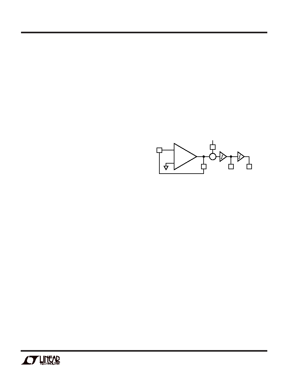
What to Do with an Unused Section
If the LTC1067 or LTC1067-50 is used as a single 2nd
order filter, the other 2nd order section is not used. Do not
leave this section unconnected. If the section is uncon-
nected, inputs and outputs are left to float to undetermined
levels and oscillation may occur. The unused section
should be connected as shown in Figure 10.
Output Voltage Swing on a Single Supply Voltage
The typical performance curves show the output voltage
swing limitations. The curves show the output signal
swing, in volts peak-to-peak, versus the output load resis-
tance. The peak-to-peak swing is limited by the following
three considerations: the op amp’s output swings closer
to the negative supply than the positive supply, the AGND
pin is biased at the midpoint of the supplies and all
operating modes are inverting.
The op amps in the LTC1067/LTC1067-50 swing closer to
the negative supply rail than the positive supply rail. The
positive output voltage swing for single supply operation
is shown in Figures 11 and 12. The negative output voltage
swing is about 15mV for the LTC1067 and 10mV for the
LTC1067-50. The negative output voltage swing is nearly
independent of load resistance since the load in this case
is connected to the V – supply rail.
For single supply applications, the on-chip resistor divider
sets the voltage at the AGND pin to the midpoint of the V +
and V – potentials. The AGND voltage is the reference for
all internal op amps. If the input to the filter is at the V – rail,
+
–
V+
∑
1067 F10
INV
HP
BP
LP
Figure 10. Connections for an Unused Section
相关PDF资料 |
PDF描述 |
|---|---|
| LTC1067CS#TRPBF | IC FILTR BLDNGBLK R-R DUAL16SOIC |
| LTC1067CS#TR | IC FILTR BLD BLK DUAL R-R 16SOIC |
| LTC1067-50CS#TRPBF | IC FILTR BLDNGBLK R-R DUAL16SOIC |
| LTC1067-50CS#TR | IC FILTR BLD BLK DUAL R-R 16SOIC |
| LTC1067-50CS | IC FILTR BLDNGBLK R-R DUAL16SOIC |
相关代理商/技术参数 |
参数描述 |
|---|---|
| LTC1067-50IS | 功能描述:IC FILTR BLDNGBLK R-R DUAL16SOIC RoHS:否 类别:集成电路 (IC) >> 接口 - 滤波器 - 有源 系列:- 产品培训模块:Lead (SnPb) Finish for COTS Obsolescence Mitigation Program 标准包装:1,000 系列:- 滤波器类型:连续时间,带通低通 频率 - 截止或中心:150kHz 滤波器数:4 滤波器阶数:8th 电源电压:4.74 V ~ 11 V,±2.37 V ~ 5.5 V 安装类型:表面贴装 封装/外壳:28-SOIC(0.295",7.50mm 宽) 供应商设备封装:28-SOIC W 包装:带卷 (TR) |
| LTC1067-50IS#PBF | 功能描述:IC FILTR BLDNGBLK R-R DUAL16SOIC RoHS:是 类别:集成电路 (IC) >> 接口 - 滤波器 - 有源 系列:- 产品培训模块:Lead (SnPb) Finish for COTS Obsolescence Mitigation Program 标准包装:1,000 系列:- 滤波器类型:连续时间,带通低通 频率 - 截止或中心:150kHz 滤波器数:4 滤波器阶数:8th 电源电压:4.74 V ~ 11 V,±2.37 V ~ 5.5 V 安装类型:表面贴装 封装/外壳:28-SOIC(0.295",7.50mm 宽) 供应商设备封装:28-SOIC W 包装:带卷 (TR) |
| LTC1067-50IS#TR | 功能描述:IC FILTR BLD BLK DUAL R-R 16SOIC RoHS:否 类别:集成电路 (IC) >> 接口 - 滤波器 - 有源 系列:- 产品培训模块:Lead (SnPb) Finish for COTS Obsolescence Mitigation Program 标准包装:1,000 系列:- 滤波器类型:连续时间,带通低通 频率 - 截止或中心:150kHz 滤波器数:4 滤波器阶数:8th 电源电压:4.74 V ~ 11 V,±2.37 V ~ 5.5 V 安装类型:表面贴装 封装/外壳:28-SOIC(0.295",7.50mm 宽) 供应商设备封装:28-SOIC W 包装:带卷 (TR) |
| LTC1067-50IS#TRPBF | 功能描述:IC FILTR BLDNGBLK R-R DUAL16SOIC RoHS:是 类别:集成电路 (IC) >> 接口 - 滤波器 - 有源 系列:- 产品培训模块:Lead (SnPb) Finish for COTS Obsolescence Mitigation Program 标准包装:1,000 系列:- 滤波器类型:连续时间,带通低通 频率 - 截止或中心:150kHz 滤波器数:4 滤波器阶数:8th 电源电压:4.74 V ~ 11 V,±2.37 V ~ 5.5 V 安装类型:表面贴装 封装/外壳:28-SOIC(0.295",7.50mm 宽) 供应商设备封装:28-SOIC W 包装:带卷 (TR) |
| LTC1067C | 制造商:LINER 制造商全称:Linear Technology 功能描述:Rail-to-Rail, Very Low Noise Universal Dual Filter Building Block |
发布紧急采购,3分钟左右您将得到回复。