- 您现在的位置:买卖IC网 > PDF目录9514 > LTC1092CN8#PBF (Linear Technology)IC DAS SERIAL I/O 1CH 10BIT 8DIP PDF资料下载
参数资料
| 型号: | LTC1092CN8#PBF |
| 厂商: | Linear Technology |
| 文件页数: | 14/32页 |
| 文件大小: | 0K |
| 描述: | IC DAS SERIAL I/O 1CH 10BIT 8DIP |
| 标准包装: | 50 |
| 类型: | 数据采集系统(DAS),ADC |
| 分辨率(位): | 10 b |
| 数据接口: | 串行 |
| 电压电源: | 双 ± |
| 电源电压: | ±5V,4.5V,10V |
| 工作温度: | -40°C ~ 85°C |
| 安装类型: | 通孔 |
| 封装/外壳: | 8-DIP(0.300",7.62mm) |
| 供应商设备封装: | 8-PDIP |
| 包装: | 管件 |
| 产品目录页面: | 1345 (CN2011-ZH PDF) |
第1页第2页第3页第4页第5页第6页第7页第8页第9页第10页第11页第12页第13页当前第14页第15页第16页第17页第18页第19页第20页第21页第22页第23页第24页第25页第26页第27页第28页第29页第30页第31页第32页
21
LTC1091/LTC1092
LTC1093/LTC1094
U
S
A
O
PPLICATI
WU
U
I FOR ATIO
3. Analog Inputs
Because of the capacitive redistribution A/D conversion
techniques used, the analog inputs of the LTC1091/
LTC1092/LTC1093/LTC1094 have capacitive switching
input current spikes. These current spikes settle quickly
and do not cause a problem. However, if large source
resistances are used or if slow settling op amps drive the
inputs, care must be taken to ensure that the transients
caused by the current spikes settle completely before the
conversion begins.
Source Resistance
The analog inputs of the LTC1091/LTC1092/LTC1093/
LTC1094 look like a 60pF capacitor (CIN) in series with a
500
resistor (RON) as shown in Figure 7. CIN gets
switched between the selected “+” and “–” inputs once
during each conversion cycle. Large external source resis-
tors and capacitances will slow the settling of the inputs. It
is important that the overall RC time constants be short
enough to allow the analog inputs to completely settle
within the allowed time.
“+” Input Settling
This input capacitor is switched onto the “+” input during
the sample phase (tSMPL, see Figure 8). The sample phase
is the 1 1/2 CLK cycles before the conversion starts. The
voltage on the “+” input must settle completely within this
sample time. Minimizing RSOURCE+ and C1 will improve
the input settling time. If large “+” input source resistance
must be used, the sample time can be increased by using
a slower CLK frequency. With the minimum possible
sample time of 3
s, RSOURCE+ < 2k and C1 < 20pF will
provide adequate settling.
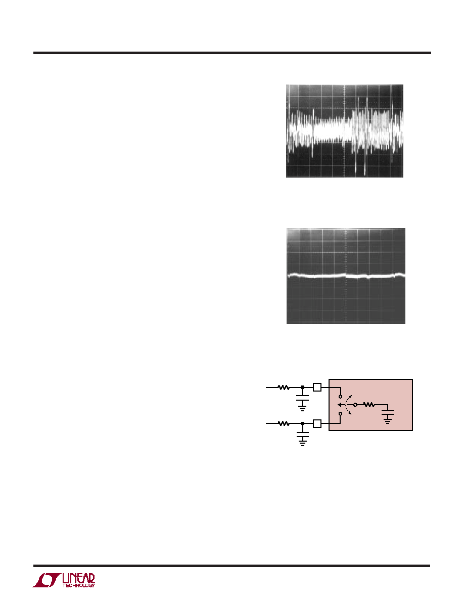
Figure 5. Poor VCC Bypassing.
Noise and Ripple Can Cause A/D Errors
10
s/DIV
1091-4 F05
0.5mV/DIV
Figure 6. Good VCC Bypassing Keeps
Noise and Ripple on VCC Below 1mV
0.5mV/DIV
10
s/DIV
1091-4 F06
3RD CLK
↑
RON = 500
4TH CLK
↓
CIN =
60pF
LTC1091
“+”
INPUT
RSOURCE+
VIN+
C1
“–”
INPUT
RSOURCE–
VIN–
C2
LTC091-4 F07
Figure 7. Analog Input Equivalent Circuit
相关PDF资料 |
PDF描述 |
|---|---|
| GTC030R-20-18P | CONN RCPT 9POS PANEL MNT W/PINS |
| V72A5M300BL2 | CONVERTER MOD DC/DC 5V 300W |
| MS3452W22-14PY | CONN RCPT 19POS BOX MNT W/PINS |
| MS3452W22-14PX | CONN RCPT 19POS BOX MNT W/PINS |
| MS3452W22-14PW | CONN RCPT 19POS BOX MNT W/PINS |
相关代理商/技术参数 |
参数描述 |
|---|---|
| LTC1092MJ8 | 制造商:未知厂家 制造商全称:未知厂家 功能描述:Analog-to-Digital Converter, 10-Bit |
| LTC1093 | 制造商:LINER 制造商全称:Linear Technology 功能描述:1-, 2-, 6- and 8-Channel, 10-Bit Serial I/O Data Acquisition Systems |
| LTC1093AC | 制造商:LINER 制造商全称:Linear Technology 功能描述:1-, 2-, 6- and 8-Channel, 10-Bit Serial I/O Data Acquisition Systems |
| LTC1093ACJ | 制造商:未知厂家 制造商全称:未知厂家 功能描述:Single-Ended Data Acquisition System |
| LTC1093ACN | 功能描述:IC DATA ACQ SYS 10BIT 6CH 16-DIP RoHS:否 类别:集成电路 (IC) >> 数据采集 - ADCs/DAC - 专用型 系列:- 产品培训模块:Lead (SnPb) Finish for COTS Obsolescence Mitigation Program 标准包装:50 系列:- 类型:数据采集系统(DAS) 分辨率(位):16 b 采样率(每秒):21.94k 数据接口:MICROWIRE?,QSPI?,串行,SPI? 电压电源:模拟和数字 电源电压:1.8 V ~ 3.6 V 工作温度:-40°C ~ 85°C 安装类型:表面贴装 封装/外壳:40-WFQFN 裸露焊盘 供应商设备封装:40-TQFN-EP(6x6) 包装:托盘 |
发布紧急采购,3分钟左右您将得到回复。